
A client spent $142 per unit on AlN ceramic substrates for an LED driver board. FR-4 with a metal-core layer would have done the job at $11. They learned this in production.
Ceramic substrate for PCB is the most over-specified and under-specified material in power electronics right now. Engineers either run from it (it’s expensive, it’s brittle, sourcing is painful) or jump to it for projects that don’t need it (a 5W LED on alumina). Both are mistakes. This article walks through where ceramic substrate PCBs actually earn their cost — and the signals that say you’ve gone too far.
Why Thermal Conductivity Alone Doesn’t Justify Ceramic Substrate PCBs
The default sales pitch for ceramic substrate PCB is thermal performance. The numbers look obvious:
- FR-4: ~0.3 W/m·K
- Aluminum-core MCPCB: ~1–3 W/m·K (limited by the dielectric layer, not the aluminum)
- Alumina (Al2O3, 96%): ~24 W/m·K
- Aluminum Nitride (AlN): ~170–180 W/m·K
- Silicon Nitride (Si3N4): ~70–90 W/m·K
So AlN moves heat roughly 560x better than FR-4. End of story?
No. Thermal conductivity is one term in a three-term chain: device-to-substrate, substrate, and substrate-to-ambient. If your TIM and heatsink dominate that chain, swapping FR-4 for AlN drops total R_th by maybe 4–7%. You just paid 12x for a 5% improvement. The substrate isn’t the bottleneck — it never was.
The case for ceramic gets real when the substrate IS the bottleneck: SiC or GaN power devices switching above 50 kHz at junction temps above 150°C, RF power amps running CW above 50W, or LED arrays with no room for an external heatsink. There, the substrate’s R_θJC sits on the critical path. Then yes — and only then — does the 10x material premium return.
CTE Mismatch: The Real Reason for AlN and Si3N4 in EV Inverters
Here’s the part most spec sheets bury. Coefficient of thermal expansion (CTE) matching matters more than raw thermal conductivity for any module that sees thermal cycling.
- Silicon: ~3 ppm/°C
- SiC: ~4 ppm/°C
- FR-4 (xy plane): ~14–17 ppm/°C
- Copper: ~17 ppm/°C
- Alumina: ~7 ppm/°C
- AlN: ~4.5 ppm/°C
- Si3N4: ~3 ppm/°C
When a SiC die is soldered to FR-4 and the system cycles between -40°C and 175°C, the differential expansion shears the solder joint. You see cracking by cycle 1,000. Move to AlN-DBC (Direct Bonded Copper on aluminum nitride) and the joint sees a fraction of the strain — but the AlN-to-copper interface is now the weak link, because copper is still at 17 ppm and AlN at 4.5.
This is why AMB-Si3N4 (Active Metal Brazed silicon nitride) has been quietly taking over 800V EV inverter substrates. We worked with a Tier-1 supplier whose AlN-DBC modules were failing power-cycling qualification at around 7,000 cycles. Switching to AMB-Si3N4 — same copper thickness, same die, same solder alloy — pushed qualification past 25,000 cycles. Substrate cost went up roughly 30%. Warranty exposure dropped enough to make it the cheapest decision they made that year.
The Four Ceramic Substrate Types and When to Pick Each
Most “ceramic PCB” datasheets blur the categories. They are not interchangeable.
Alumina (Al2O3) Thick or Thin Film
The workhorse. ~24 W/m·K, lowest cost in the ceramic family, available in 96% and 99.6% purities. Use this for: LED arrays under 50W per board, RF up to ~10 GHz where Dk variation is acceptable, automotive sensors, hybrid microelectronics. Don’t use it when you need either >50 W/m·K conduction or tight CTE matching to silicon.
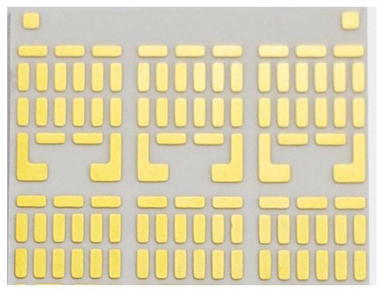
Aluminum Nitride (AlN) DBC
The best thermal conductivity in mass production. The catch: AlN is hygroscopic at the surface and prone to micro-cracking during DBC processing. Yield runs 70–85% at reputable fabs, which is why your quote came back at $90+ per panel.
Silicon Nitride (Si3N4) AMB
The mechanical toughness winner. Flexural strength ~700–900 MPa versus AlN at ~300–400 MPa. This is the substrate that survives 25,000+ power cycles in EV traction inverters. Cost: roughly 1.3–1.6x AlN. Expect 6–10 week lead times — there are only a handful of qualified suppliers globally.
LTCC and HTCC for RF and Microwave
Multilayer co-fired ceramics. LTCC fires at 850–900°C and can integrate silver conductors, capacitors, and resistors inside the stack-up. HTCC fires above 1,500°C and uses refractory metals like tungsten. For phased-array radar, mmWave front-ends, and aerospace transponders, this is where the design lives. It is not a “PCB” in any way an FR-4 designer would recognize.
A 6-Point Decision Framework Before You Spec Ceramic Substrate PCBs
Before signing the BOM, walk through these six questions. If fewer than three point to ceramic, you don’t need ceramic.
- Is the device junction temperature staying above 150°C in normal operation, not just worst-case?
- Is the substrate’s R_θJC the limiting term in your thermal chain (verified by an actual thermal sim, not a hunch)?
- Is the CTE mismatch between die and standard PCB causing solder joint failure in qualification?
- Is operating frequency above 5–10 GHz with insertion loss budgets tighter than 0.5 dB/inch?
- Are you in an environment where outgassing, ITAR, or aerospace qualification rules out organic laminates?
- Does the volume justify the tooling — ceramic NRE for custom sizes can run $8K–$20K?
If you said yes to three or more, ceramic earns its place. If you said yes to one or two, you probably want a hybrid solution — an IMS (Insulated Metal Substrate) board with a small ceramic carrier under the hot die only. That’s the design we end up at 60% of the time.
Most projects that “need” ceramic actually need better thermal design on FR-4 — and most projects on FR-4 that should be ceramic are still on FR-4 because nobody ran the cycle-life math.
Common Mistakes Engineers Make with Ceramic Substrate PCB Sourcing
Five errors we see every quarter:
- Specifying AlN when alumina would work. Alumina is roughly 25% of AlN cost. Half the LED projects asking for AlN run flux densities under 8 W/cm² — alumina handles that all day.
- Ignoring the metallization spec. “Ceramic PCB, 0.5 oz copper” is meaningless. Is it DBC (thick, etched, coarse features), DPC (thin film plus electroplate, fine features down to 50 µm lines/spaces), or thick-film printed (cheap, ~150 µm minimum)? Each has different current capacity, resolution, and reliability behavior.
- Forgetting surface finish reality. ENIG on ceramic-DPC is standard. ENIG on DBC needs careful process control — porosity issues are common. We’ve seen black-pad failures on DBC-ENIG that wouldn’t show up in standard IPC-4552 testing because that spec was written around organic substrates.
- Designing edge-routed when scoring would work — or vice versa. Ceramic is brittle. V-cut depaneling on alumina cracks 5–15% of boards. Laser scribing or full singulation is required, and that adds $1–3 per piece. Build it into the quote, not the surprise invoice.
- Skipping the partial-discharge test. For any board above 1 kV — EV traction, grid-tie inverter, X-ray — partial discharge testing per IEC 60664 is non-negotiable. FR-4 fails this consistently above 1.5 kV across reasonable creepage. Ceramic passes, but only if your metallization edges are properly chamfered.
Are you still defaulting to FR-4 plus heatsink for GaN designs above 100 kHz? What’s driving that choice — cost, sourcing comfort, or actual thermal data?
How to Source Ceramic Substrate PCB Without Getting Burned
Three Monday-morning actions:
- Get DPC and DBC quotes side by side. Most engineers ask for one or the other. The comparison reveals where your design has been over-spec’d.
- Ask the fab for their typical yield on your panel size and minimum trace width. If they won’t share, that’s data too.
- Pull IPC-A-600 Class 2 vs Class 3 acceptability criteria for your trace geometry, then ask the supplier to confirm in writing which class they will meet. Ceramic suppliers default to Class 2 even when your application needs Class 3.
Ceramic substrate for PCB is not a premium upgrade. It is a specific tool for specific thermal, electrical, and mechanical envelopes. Spec it for the right reason and it pays back fast. Spec it because the datasheet looked impressive and you’ve added $130 per board for a 5% improvement in something that wasn’t actually broken.
What’s the one substrate decision in your last design that you would reverse with what you know now?


Leave a Reply