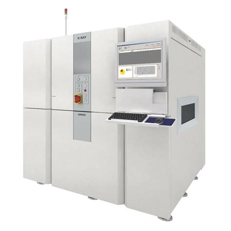
What is AXI Technology?
Automated X-Ray Inspection (AXI) is a non-destructive testing method that uses X-rays to inspect the internal structure of PCBs. This technology allows for the detection of defects that are not visible to the naked eye or other optical inspection methods. AXI systems use high-resolution X-ray imaging to create detailed 2D and 3D images of the PCB, which are then analyzed by advanced software algorithms to identify any potential issues.
How does AXI Technology work?
AXI systems consist of three main components: an X-ray source, an X-ray detector, and a computer system with specialized software. The process begins with the PCB being placed in the inspection chamber. The X-ray source then emits a beam of X-rays that passes through the PCB and is captured by the detector on the opposite side. The detector converts the X-rays into a digital image, which is then processed by the computer system using advanced algorithms to identify any defects or anomalies.
Advantages of AXI Technology over traditional inspection methods
| Traditional Inspection Methods | AXI Technology |
|---|---|
| Limited to surface-level defects | Can detect internal defects |
| Time-consuming manual process | Automated, high-speed inspection |
| Subjective, prone to human error | Objective, consistent results |
| Destructive testing may be required | Non-destructive testing |
Benefits of using AXI Technology in PCB Assembly
1. Improved defect detection
One of the primary benefits of using AXI technology in PCB assembly is its ability to detect a wide range of defects that may not be visible using other inspection methods. These defects can include:
- Solder joint defects (voids, bridges, insufficient solder)
- Component placement issues
- Broken or missing components
- PCB warpage or delamination
- Trace or via defects
By detecting these defects early in the assembly process, manufacturers can avoid costly rework or product failures in the field.
2. Increased efficiency and productivity
AXI systems are highly automated, allowing for faster inspection times compared to manual methods. This increased efficiency translates to higher throughput and lower production costs. Additionally, the objective nature of AXI inspection eliminates the subjectivity and variability associated with human inspectors, ensuring consistent results across multiple PCBs.
3. Non-destructive testing
Unlike some traditional inspection methods that may require destructive testing, AXI is a non-destructive technique. This means that PCBs can be inspected without causing any damage, allowing for 100% inspection of all assembled boards. Non-destructive testing is particularly valuable for high-value or mission-critical applications where product reliability is of utmost importance.
4. Improved product quality and reliability
By detecting defects early in the assembly process, AXI technology helps manufacturers ensure the highest level of product quality and reliability. This, in turn, leads to reduced warranty claims, improved customer satisfaction, and a stronger brand reputation. In industries where product failure can have serious consequences, such as aerospace or medical devices, the use of AXI technology is essential for maintaining the highest standards of quality and safety.
5. Cost savings
While the initial investment in AXI equipment may be higher than traditional inspection methods, the long-term cost savings can be significant. By catching defects early and reducing the need for rework or scrap, manufacturers can minimize production costs and improve overall profitability. Additionally, the increased efficiency and productivity offered by AXI technology can help reduce labor costs and improve overall equipment effectiveness (OEE).

Applications of AXI Technology
AXI technology is widely used across various industries that rely on PCB assembly, including:
- Aerospace and defense
- Automotive
- Medical devices
- Telecommunications
- Consumer electronics
In each of these industries, the use of AXI technology helps ensure the highest levels of product quality, reliability, and safety.

Implementing AXI Technology in your PCB Assembly Process
If you are considering implementing AXI technology in your PCB assembly process, there are several factors to keep in mind:
- Choose the right AXI system for your needs, considering factors such as PCB complexity, production volume, and budget.
- Develop a comprehensive inspection plan that defines the specific defects to be detected and the acceptance criteria for each.
- Train your operators on the proper use and maintenance of the AXI equipment.
- Integrate AXI inspection into your overall quality control process, ensuring that defects are properly documented and addressed.
- Continuously monitor and optimize your AXI process to ensure maximum efficiency and effectiveness.
By following these steps, you can successfully implement AXI technology in your PCB assembly process and reap the many benefits it has to offer.

Frequently Asked Questions (FAQ)
1. What types of defects can AXI technology detect?
AXI technology can detect a wide range of defects, including solder joint defects (voids, bridges, insufficient solder), component placement issues, broken or missing components, PCB warpage or delamination, and trace or via defects.
2. Is AXI technology suitable for all types of PCBs?
AXI technology is suitable for most types of PCBs, including those with high component density, complex geometries, or multi-layer designs. However, very thick PCBs or those with dense, high-Z materials may pose challenges for X-ray inspection.
3. How does AXI technology compare to automated optical inspection (AOI)?
While AOI is effective for detecting surface-level defects, AXI technology can detect both surface and internal defects. AXI is particularly useful for inspecting solder joints, which are often obscured from view in optical inspection methods.
4. Is AXI technology safe for operators?
Yes, modern AXI systems are designed with operator safety in mind. The X-ray radiation is contained within the inspection chamber, and the systems are equipped with safety interlocks to prevent accidental exposure.
5. What is the typical return on investment (ROI) for implementing AXI technology?
The ROI for implementing AXI technology can vary depending on factors such as production volume, PCB complexity, and the cost of defects. However, many manufacturers report significant cost savings and quality improvements after implementing AXI, with some seeing ROI within the first year of operation.
Conclusion
In the competitive world of PCB assembly, choosing the right inspection technology can make all the difference in ensuring product quality, reliability, and customer satisfaction. Automated X-Ray Inspection (AXI) technology offers a powerful solution for detecting a wide range of defects, improving efficiency and productivity, and reducing overall production costs. By implementing AXI technology in your PCB assembly process, you can take your quality control to the next level and stay ahead of the competition.


Leave a Reply