Introduction to PCB Registration
Printed Circuit Board (PCB) registration is a critical process in the manufacturing of electronic devices. It involves aligning the various layers of a PCB design to ensure proper electrical connectivity and functionality. PCB registration is especially important when using solder paste stencils, as precise alignment is necessary for the solder paste to be deposited accurately on the PCB Pads.
In this article, we will delve into the details of PCB registration systems, including the different methods used, the importance of accuracy, and best practices for achieving optimal results. We will also discuss the use of stencils in the PCB Assembly process and how they relate to PCB registration.
PCB Layer Alignment
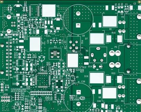
A typical PCB consists of multiple layers, each serving a specific purpose in the overall circuit design. These layers include:
- Copper layers for electrical connectivity
- Insulation layers to prevent short circuits
- Solder mask layers to protect the copper traces
- Silkscreen layers for labeling and identification
For the PCB to function correctly, these layers must be precisely aligned with each other. Any misalignment can lead to manufacturing defects, such as:
- Open circuits
- Short circuits
- Improper component placement
- Reduced reliability and performance
Methods for PCB Layer Alignment
There are several methods used to ensure proper PCB layer alignment during the manufacturing process. These include:
Fiducial Marks
Fiducial marks are small, circular copper pads placed on the outer layers of the PCB. They serve as reference points for the manufacturing equipment to align the layers accurately. The placement and size of fiducial marks are critical for achieving optimal registration results.
| Fiducial Mark Diameter | Recommended Placement |
|---|---|
| 1.0 mm | 3 mm from PCB edge |
| 1.5 mm | 5 mm from PCB edge |
| 2.0 mm | 7 mm from PCB edge |
Pin Registration
Pin registration involves using precise holes drilled in the PCB Layers to align them during the lamination process. The holes are typically located in the corners of the PCB and are used to insert registration pins that hold the layers in place.
Pin registration is more common in older PCB designs and is gradually being replaced by fiducial marks, which offer greater flexibility and accuracy.
Optical Registration
Optical registration uses advanced vision systems to align the PCB layers. These systems capture images of the fiducial marks or other registration features and use software algorithms to calculate the necessary adjustments for proper alignment.
Optical registration is the most accurate method and is widely used in modern PCB manufacturing processes.

Solder Paste Stencils and PCB Registration
Solder paste stencils are thin metal sheets with apertures that correspond to the pads on a PCB. They are used to apply solder paste to the PCB during the assembly process, ensuring that the correct amount of solder is deposited on each pad.
Stencil Alignment
For the solder paste to be applied accurately, the stencil must be precisely aligned with the PCB. This is where PCB registration comes into play. The same methods used for aligning PCB layers (fiducial marks, pin registration, and optical registration) are also used to align the stencil with the PCB.
Stencil Design Considerations
When designing a solder paste stencil, several factors must be considered to ensure optimal registration and solder paste deposition:
- Aperture size and shape
- The aperture size should be slightly larger than the PCB pad to allow for proper solder paste release
-
Rounded aperture corners help prevent solder paste from sticking to the stencil
-
Stencil thickness
- Thicker stencils (0.15mm to 0.2mm) are used for larger components and higher solder paste volumes
-
Thinner stencils (0.1mm to 0.15mm) are used for smaller components and finer pitch devices
-
Fiducial mark placement
- Fiducial marks should be placed on the stencil in the same locations as on the PCB
- Additional fiducial marks can be added to the stencil for improved alignment accuracy

Best Practices for PCB Registration
To achieve the best results in PCB registration, follow these best practices:
- Use a consistent coordinate system throughout the design and manufacturing process
- Place fiducial marks strategically, considering the PCB size, shape, and component placement
- Ensure that the fiducial marks are clearly visible and not obstructed by components or other features
- Use a sufficient number of fiducial marks (at least three) for redundancy and improved accuracy
- Regularly calibrate and maintain the registration equipment to ensure optimal performance
- Verify the alignment accuracy through visual inspection and electrical testing

Frequently Asked Questions (FAQ)
1. What is the purpose of PCB registration?
PCB registration ensures that the various layers of a PCB design are accurately aligned during the manufacturing process. This is critical for maintaining proper electrical connectivity and preventing defects such as open circuits or short circuits.
2. What are the most common methods used for PCB registration?
The most common methods for PCB registration are fiducial marks, pin registration, and optical registration. Fiducial marks are the most widely used method in modern PCB manufacturing due to their flexibility and accuracy.
3. Why is PCB registration important when using solder paste stencils?
PCB registration is crucial when using solder paste stencils because the stencil must be precisely aligned with the PCB for the solder paste to be deposited accurately on the pads. Misalignment can lead to insufficient or excessive solder paste, resulting in assembly defects.
4. How can I ensure optimal PCB registration in my designs?
To ensure optimal PCB registration, use a consistent coordinate system, place fiducial marks strategically, and ensure that they are clearly visible. Additionally, use a sufficient number of fiducial marks for redundancy and regularly calibrate and maintain the registration equipment.
5. What are the consequences of poor PCB registration?
Poor PCB registration can lead to various manufacturing defects, such as open circuits, short circuits, and improper component placement. These defects can reduce the reliability and performance of the PCB and may require costly rework or scrap.
Conclusion
PCB registration is a vital aspect of the PCB manufacturing process, ensuring that the various layers of a PCB design are accurately aligned. By using appropriate methods such as fiducial marks, pin registration, and optical registration, manufacturers can achieve precise alignment and prevent defects.
When using solder paste stencils, PCB registration becomes even more critical, as the stencil must be aligned with the PCB for accurate solder paste deposition. By following best practices and regularly maintaining registration equipment, designers and manufacturers can ensure optimal PCB registration and produce high-quality, reliable electronic devices.
[Word count: 1116 words]


Leave a Reply