
THE CERAMIC CIRCUIT ENGINEERING RESOURCE
Ceramic PCB.
Start with the
right substrate.
Better circuits begin with better material decisions. Compare ceramics, understand the process and work through the numbers before you build.
Al₂O₃ · AlN · Si₃N₄ · DBC · DPC · AMB · LTCC · HTCC
01 / MATERIAL SELECTION
Different ceramics.
Different engineering priorities.
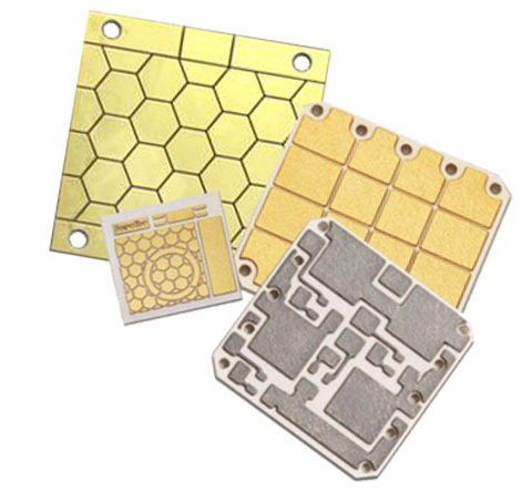
A ceramic PCB uses an inorganic substrate to support and electrically isolate its conductors. The right grade depends on the complete circuit and heat path.
Alumina
Cost-conscious thermal isolation
DBC · DPC · thick filmAlNAluminum nitride
Low substrate thermal resistance
DBC · DPC · AMBSi₃N₄Silicon nitride
Mechanical and cycling robustness
AMBZTAZirconia-toughened alumina
Toughened alumina power substrates
DBCNamed product examples at 20°C from Rogers curamik material data. These are reference values, not guaranteed properties for all grades. See grades and conditions.
02 / THE ENGINEERING WORKBENCH
Make the cost assumptions visible.
Explore how size, quantity and process yield change a ceramic PCB cost scenario. Replace the illustrative rates with your project data.
03 / DESIGN NOTES
Design for the whole assembly.
A high-conductivity substrate is a starting point. Copper geometry, interfaces, mounting and process control turn it into a useful circuit.
Ceramic PCB thermal design: follow the heat path
A ceramic PCB is one part of a heat-transfer system. Add the resistance of the die, attachment layers, substrate, thermal interface and cooler before estimating device temperature.
Read the guide02 / Design guidesCopper thickness on ceramic PCBs
Copper thickness affects electrical resistance, heat spreading, patterning and mechanical stress. Choose it with conductor width and manufacturing process rather than treating thicker copper as an automatic upgrade.
Read the guide03 / Design guidesCreepage, clearance and ceramic PCB insulation
Ceramic bulk dielectric strength does not determine safe working voltage for a finished circuit. Insulation design also depends on geometry, interfaces, environment and the applicable product standard.
Read the guide04 / Design guidesVias and holes in ceramic circuit boards
Ceramic holes can provide electrical interconnect, mechanical location or a thermal path. State their purpose because each function creates different manufacturing and inspection requirements.
Read the guide05 / Design guidesMounting and handling ceramic circuit boards
Ceramic substrates are stiff and brittle. Design supports, fixtures and fastening loads so the circuit is not forced to accommodate bending or concentrated edge impacts.
Read the guide06 / Design guidesCeramic PCB DFM checklist
A useful ceramic PCB manufacturability review checks the exact material, process, drawing, assembly method and acceptance tests. Resolve conflicting requirements before requesting production pricing.
Read the guide04 / CIRCUIT CONSTRUCTIONS
From a substrate to a product.
Ceramic power substrates
Ceramic power substrates combine electrically isolated circuits with a heat path from semiconductor devices to the cooling assembly. DBC and AMB are important construction families.
Read the guide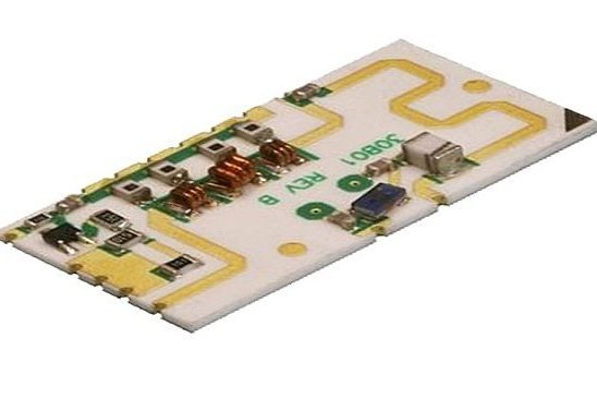
Ceramic hybrid circuits
Hybrid circuits combine printed or deposited functions with attached components on a ceramic carrier. Thick-film and thin-film approaches offer different routes to integration and precision.
Read the guide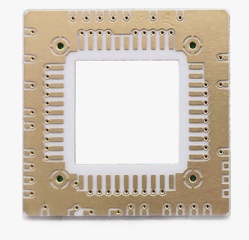
Hermetic ceramic electronic packages
A hermetic ceramic package combines a ceramic body, electrical feedthroughs and a sealing system. The completed package, rather than the bare substrate, must meet the specified leak and environmental requirements.
Read the guideOriginal project-supplied photographs illustrate circuit formats. A photo does not verify ceramic composition, hidden layers or manufacturing process.
05 / PROCESS SELECTION
Material and process are two separate decisions.
Alumina and AlN describe the ceramic. DBC, DPC and AMB describe how a metal circuit is formed or joined. LTCC and HTCC describe co-fired multilayer systems.
When should I compare DBC and AMB?
When power-circuit copper, electrical isolation and thermal cycling drive the construction. Compare the complete copper/ceramic system and its qualification evidence.
When is DPC worth evaluating?
When plated conductor geometry, fine pads or metallized ceramic holes are important. Confirm the combination of thickness, spacing and via geometry with the manufacturer.
When do LTCC and HTCC fit?
When internal routing, cavities, vias or package integration call for a co-fired multilayer structure. Tape, conductors and firing behavior are selected as a system.
06 / QUICK ANSWERS
Common ceramic PCB questions.
Begin with a clear requirement, then use the linked guides to check the details.
Browse the ceramic PCB FAQIs a ceramic PCB always better than FR-4?
No. Ceramic can help with thermal isolation, dimensional stability and package requirements, while FR-4 remains appropriate for many complex and economical circuits. Compare the complete design, not just substrate conductivity.
Does aluminum nitride always run cooler?
It can lower resistance through the substrate. Device temperature also depends on interfaces, heat spreading and cooling. An interface-dominated stack may see only a small benefit.
How much does a ceramic PCB cost?
Material grade, area, process, copper, tolerances, yield and setup all contribute. The cost tool exposes an illustrative model; an actual quotation needs a released drawing and supplier review.
Can ceramic PCBs be multilayer?
Yes. LTCC and HTCC create co-fired multilayers, while other ceramic constructions can use qualified dielectric and interconnect systems. Specify the exact structure and process.
FROM REQUIREMENT TO REVIEW
Make your next design decision concrete.
Put your material, stack-up and acceptance requirements into a project brief, then discuss the details with Judy.