
Partition the circuit by function
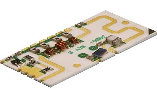
Printed resistors, conductor networks, bare dies and packaged components can share a substrate. Decide which functions benefit from printing or deposition and which should remain discrete. Include trimming access and test points in the layout.
Manage the process sequence
Firing, trimming, plating, attachment and wire bonding create a sequence of thermal and surface exposures. Select compatible materials and specify the order. A later process must not damage a previously qualified resistor, pad or joint.
Specify electrical stability
Initial tolerance is only one requirement. Resistor drift, temperature coefficient, leakage and environmental behavior may matter more in operation. Use representative witness structures and functional tests after the agreed processing and aging steps.
Engineering example
A sensor amplifier with trimmed resistors should be characterized after final attachment and cleaning, because those steps can shift performance from the values measured immediately after trimming.
Before you release the design
- Identify printed, deposited and attached functions.
- Define trim and test access.
- Qualify the complete process sequence.
Sources and further technical reading
Manufacturer references support the material and process context. Worked examples and checklists are engineering guidance; they are not test results or supplier guarantees.