
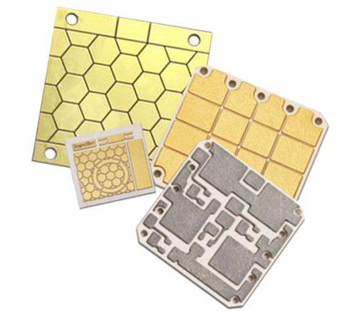
Specify the entire power path
Current enters through terminals, spreads through copper and reaches the devices through attachment interfaces. Model constrictions and local losses, not just average copper area. The ceramic, bottom metal and cooler then form the heat-removal path.
Select insulation and mechanical margin together
Alumina, AlN, ZTA and silicon nitride offer different trade-offs. Ceramic thickness must satisfy the relevant electrical and mechanical requirements. A thinner substrate can lower thermal resistance but changes handling and insulation design.
Qualify the assembled module
The substrate is only one potential failure location. Die attach, wire bonds, terminals, encapsulation and cooling interfaces also need review. Compare candidates with relevant power cycling, temperature cycling and electrical tests using the same mission profile.
Engineering example
A copper island with a narrow neck may create both current crowding and a temperature hot spot. Improve geometry before assuming a higher-conductivity ceramic alone will solve the problem.
Before you release the design
- Provide device locations, current paths and losses.
- Define working voltage and package construction.
- Specify relevant reliability and inspection requirements.
Sources and further technical reading
Manufacturer references support the material and process context. Worked examples and checklists are engineering guidance; they are not test results or supplier guarantees.