
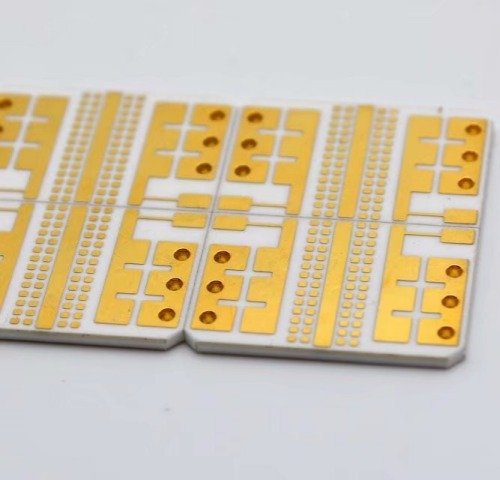
Choose AlN when it changes the system result
A higher conductivity substrate cannot repair a thick, poorly applied thermal interface or an undersized heat sink. Compare identical die area, ceramic thickness and boundary conditions before assigning value to AlN. Model temperature-dependent properties when the operating temperature differs substantially from the data-sheet test condition.
Match the metallization route
AlN can be used in several circuit and package constructions. DPC supports plated conductors; DBC or AMB supports power substrates; selected grades also support specialist thin-film or co-fired structures. Process compatibility is supplier-specific. Specify the purchased structure rather than assuming all AlN grades accept the same processing.
Control assembly interfaces
Low ceramic CTE helps some die attachments, but the copper-clad assembly has a different effective expansion. Large solder joints, connectors and heat sinks can still introduce stress. Confirm cleaning compatibility, storage conditions, bond-pad metallurgy and thermal-cycling evidence for the final assembly.
Engineering example
Using k = 170 W/m·K, a 0.635 mm AlN layer over 100 mm² contributes about 0.0374 K/W in a one-dimensional model. The same dimensions with k = 24 give 0.265 K/W. The difference belongs to the ceramic layer only.
Before you release the design
- Use thermal conductivity at the relevant temperature.
- Specify copper, ceramic and interface thickness separately.
- Review the supplier’s handling and cleaning instructions.
Sources and further technical reading
Manufacturer references support the material and process context. Worked examples and checklists are engineering guidance; they are not test results or supplier guarantees.