
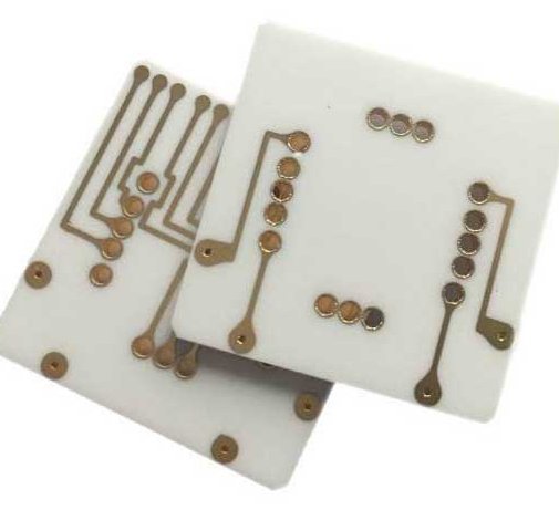
Where alumina fits
Use alumina as the baseline in a material study for hybrids, sensors, LED carriers and many power substrates. It can carry printed thick-film circuits, deposited thin films or bonded copper. These constructions are different products: an alumina specification alone does not determine copper thickness, feature size or assembly compatibility.
Read the grade, not just the chemical formula
Purity, additives, grain structure and surface finish influence the finished substrate. A polished thin-film grade and an as-fired thick-film grade should not be substituted on purity alone. Ask for roughness, flatness and the thermal conductivity of the purchased grade. The material comparison table uses a named 24 W/m·K product example, not a guaranteed value for every alumina board.
Establish the thermal and mechanical limits
Calculate the ceramic contribution to thermal resistance, then include die attach, copper spreading, the thermal interface and the cooling assembly. Alumina is brittle: provide support under assembly loads, control edge damage and avoid treating a high flexural-strength value as permission to bend the board. If ceramic resistance dominates, compare a thinner qualified construction or AlN. If cracking dominates, compare ZTA or Si₃N₄.
Engineering example
For a 0.635 mm ceramic layer and a 100 mm² ideal heat-flow area, k = 24 W/m·K gives R = 0.265 K/W. This excludes spreading and interfaces; it is a screening calculation, not a device junction temperature.
Before you release the design
- Specify alumina grade and surface condition.
- Choose the metallization route and finished conductor dimensions.
- Verify thickness, insulation and assembly support together.
Sources and further technical reading
Manufacturer references support the material and process context. Worked examples and checklists are engineering guidance; they are not test results or supplier guarantees.