
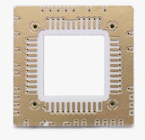
Treat the package as a multi-material assembly
Cofired vias, external metallization, leads, seal rings and lids create multiple interfaces. Each must be compatible with the joining sequence and thermal expansion of the surrounding materials. A cavity in a ceramic board is not by itself a hermetic enclosure.
Design functional interfaces together
Electrical routing, thermal attachment, optical windows and mechanical datums may compete for space. Define these requirements in a package drawing and review tolerances after all joining steps. Include lid clearance and wire-loop height where applicable.
Specify finished-package verification
Define the leak-test method, acceptance criteria and test stage in the purchasing requirements. Include electrical and environmental tests appropriate to the device. Traceability should connect ceramic, metallization and sealing process revisions to the delivered package.
Engineering example
A package can pass electrical continuity before sealing and fail after lid attachment because of mechanical or thermal effects. Repeat the relevant functional checks at the completed-package stage.
Before you release the design
- Define feedthrough, lid and seal interfaces.
- Specify the final leak-test requirements.
- Control materials and assembly process revisions.
Sources and further technical reading
Manufacturer references support the material and process context. Worked examples and checklists are engineering guidance; they are not test results or supplier guarantees.