Overview of PCB Visualizer
PCB Visualizer is a software application that offers a user-friendly interface for designing and visualizing PCBs. It enables users to create complex PCB layouts, view them in 3D, and perform various analyses to ensure optimal performance and manufacturability.
Key Features of PCB Visualizer
- Schematic Capture
- PCB Layout Design
- 3D Visualization
- Design Rule Checking (DRC)
- Automatic Routing
- Bill of Materials (BOM) Generation
- Gerber File Output
Benefits of Using PCB Visualizer
Using PCB Visualizer offers several benefits to engineers and designers involved in PCB design projects:
- Increased Efficiency
- Improved Design Quality
- Enhanced Collaboration
- Cost Savings
- Faster Time-to-Market

Getting Started with PCB Visualizer
To get started with PCB Visualizer, follow these steps:
- Download and Install PCB Visualizer
- Create a New Project
- Design Your Schematic
- Create Your PCB Layout
- Perform Design Rule Checks
- Generate Manufacturing Files
System Requirements
Before installing PCB Visualizer, ensure that your system meets the following minimum requirements:
| Component | Minimum Requirement |
|---|---|
| Operating System | Windows 7, macOS 10.12, or Linux (64-bit) |
| Processor | Intel Core i5 or equivalent |
| RAM | 8 GB |
| Storage | 5 GB free space |
| Display | 1920 x 1080 resolution |

PCB Design Workflow with PCB Visualizer
The typical PCB design workflow using PCB Visualizer involves the following steps:
- Schematic Design
- Component Placement
- Routing
- Design Rule Checking
- 3D Visualization
- Manufacturing File Generation
Schematic Design
In PCB Visualizer, the schematic design process involves creating a graphical representation of the electronic circuit. This includes adding components, connecting them with wires, and defining their properties.
Creating a New Schematic
To create a new schematic in PCB Visualizer:
- Click on the “New Schematic” button in the main toolbar
- Select the schematic size and orientation
- Add components from the library or create custom components
- Connect components using wires or buses
- Define component properties, such as values and footprints
Component Placement
Once the schematic design is complete, the next step is to place the components on the PCB layout. PCB Visualizer provides tools for manual and automatic component placement.
Manual Component Placement
To manually place components on the PCB layout:
- Switch to the PCB layout view
- Select the component from the schematic or the component list
- Place the component on the desired location on the PCB
- Rotate and adjust the component as needed
Automatic Component Placement
PCB Visualizer also offers automatic component placement functionality:
- Define placement constraints, such as component grouping and keep-out areas
- Run the automatic placement tool
- Review and adjust the placement results if necessary
Routing
After component placement, the next step is to route the connections between the components. PCB Visualizer provides both manual and automatic routing options.
Manual Routing
To manually route connections:
- Select the desired routing layer
- Choose the appropriate routing width
- Start routing from a component pin or a via
- Continue routing until reaching the target pin or via
- Add vias as needed to change layers
Automatic Routing
PCB Visualizer’s automatic routing feature can save time and effort:
- Define routing constraints, such as via styles and routing preferences
- Select the connections to be routed
- Run the automatic router
- Review and adjust the routing results if necessary
Design Rule Checking
Design Rule Checking (DRC) is an essential step in the PCB design process to ensure that the design meets the required manufacturing and electrical constraints. PCB Visualizer includes a comprehensive DRC tool.
Running Design Rule Checks
To run design rule checks in PCB Visualizer:
- Define the design rules, such as minimum clearances and trace widths
- Select the desired rule set
- Run the DRC tool
- Review the DRC results and address any violations
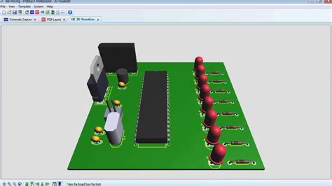
3D Visualization
PCB Visualizer provides a powerful 3D visualization feature that allows you to view your PCB design in a realistic, three-dimensional representation.
Viewing Your Design in 3D
To view your PCB design in 3D:
- Switch to the 3D view
- Adjust the camera position and orientation
- Apply realistic materials and textures to the components and PCB
- Inspect the design for potential issues, such as component clearance and mechanical fit
Manufacturing File Generation
Once your PCB design is complete and has passed the necessary design rule checks, you can generate the manufacturing files required for production.
Generating Gerber Files
To generate Gerber files in PCB Visualizer:
- Select the desired Gerber file format and settings
- Choose the layers to be included in the output
- Define the aperture settings
- Generate the Gerber files
- Review the generated files for accuracy
Generating Drill Files
To generate drill files:
- Select the desired drill file format and settings
- Define the drill sizes and tolerances
- Generate the drill files
- Review the generated files for accuracy

Advanced Features of PCB Visualizer
PCB Visualizer offers several advanced features that can further enhance your PCB design experience:
Scripting and Automation
PCB Visualizer supports scripting and automation using Python, allowing you to automate repetitive tasks and create custom functionality.
Creating Scripts
To create scripts in PCB Visualizer:
- Open the integrated development environment (IDE) for scripting
- Write your script using Python
- Test and debug your script
- Run the script to automate tasks or add custom features
Simulation and Analysis
PCB Visualizer includes built-in simulation and analysis tools to help you optimize your PCB design for electrical performance and signal integrity.
Signal Integrity Analysis
To perform signal integrity analysis:
- Define the signal nets and constraints
- Set up the simulation parameters
- Run the signal integrity analysis
- Review the results and make necessary adjustments to your design
Thermal Analysis
To perform thermal analysis:
- Define the thermal constraints and heat sources
- Set up the simulation parameters
- Run the thermal analysis
- Review the results and optimize your design for thermal performance
Collaborative Design
PCB Visualizer supports collaborative design, allowing multiple team members to work on the same PCB design project simultaneously.
Sharing Design Files
To share design files with your team:
- Set up a shared repository or cloud storage
- Upload your design files to the shared location
- Invite team members to access the shared files
- Collaborate on the design, with each team member working on their assigned tasks
Version Control
PCB Visualizer integrates with version control systems, such as Git, to manage design revisions and track changes.
To use version control with PCB Visualizer:
- Set up a version control repository for your project
- Commit your design files to the repository
- Create branches for different design versions or experiments
- Merge branches and resolve conflicts as needed
- Tag important milestones or releases
Frequently Asked Questions (FAQ)
- Q: What are the system requirements for running PCB Visualizer?
A: The minimum system requirements for PCB Visualizer are: - Operating System: Windows 7, macOS 10.12, or Linux (64-bit)
- Processor: Intel Core i5 or equivalent
- RAM: 8 GB
- Storage: 5 GB free space
-
Display: 1920 x 1080 resolution
-
Q: Does PCB Visualizer support automatic routing?
A: Yes, PCB Visualizer includes an automatic routing feature that can route connections between components based on predefined constraints and preferences. -
Q: Can I create custom components in PCB Visualizer?
A: Yes, PCB Visualizer allows you to create custom components by defining their schematic symbols, footprints, and 3D models. -
Q: Does PCB Visualizer support collaborative design?
A: Yes, PCB Visualizer supports collaborative design by allowing multiple team members to work on the same design files simultaneously, with the help of shared repositories and version control systems. -
Q: Can I automate tasks in PCB Visualizer using scripting?
A: Yes, PCB Visualizer supports scripting and automation using Python, enabling you to automate repetitive tasks and create custom functionality.
Conclusion
PCB Visualizer is a comprehensive and powerful tool for designing, visualizing, and analyzing printed circuit boards. With its user-friendly interface, advanced features, and streamlined workflow, PCB Visualizer empowers engineers and designers to create high-quality PCB designs efficiently.
By following the steps outlined in this article, you can effectively utilize PCB Visualizer to design schematics, place components, route connections, perform design rule checks, visualize your design in 3D, and generate manufacturing files.
Moreover, PCB Visualizer’s advanced features, such as scripting, simulation, and collaborative design, further enhance its capabilities and adaptability to various project requirements.
Whether you are a beginner or an experienced PCB designer, PCB Visualizer provides the tools and functionality needed to streamline your design process and achieve optimal results.


Leave a Reply