What is PCB Assembly?
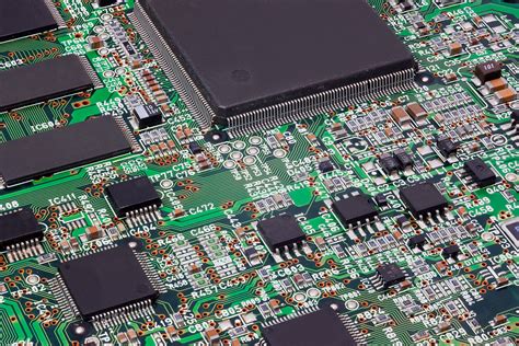
PCB assembly, or PCBA, is the process of soldering or mounting electronic components to a printed circuit board (PCB). The PCB provides the conductive pathways between components. PCB assembly turns the bare board into a functional electronic device ready for installation in an end product.
PCBA is used for prototypes, small production runs, and large volume manufacturing of electronic devices. It’s a core service provided by Electronics Manufacturing Services (EMS) companies.
The PCB Assembly Process
The PCB assembly process generally follows these steps:
-
Solder Paste Application: Solder paste (a mix of tiny metal balls and flux) is precisely applied to the board pads using a stencil.
-
Component Placement: The surface mount components are placed onto the solder paste deposits using pick-and-place machines. Complex boards may use several machines optimized for different component sizes.
-
Reflow Soldering: The PCB passes through a reflow oven which melts the solder, permanently attaching the components to the board. The oven temperature profile is carefully controlled.
-
Inspection: Automated optical inspection (AOI) checks for missing components, tombstoning, bridging, and other defects. X-ray inspection may be used for BGA and other hidden solder joints.
-
Through-hole Assembly: Any through-hole components are now inserted, often by hand. Wave soldering or selective soldering is then used to solder the component leads in place.
-
Cleaning and Coating: Residues are cleaned off, and conformal coating may be applied to protect the board from moisture and contaminants.
-
Final Test: The board functionality is comprehensively tested and boards are packaged for shipment.
Many of these steps are automated for speed, precision and repeatability, especially in high volume production. However, prototypes and small runs rely more on skilled human operators.

PCB Assembly Services for Prototypes
Getting PCB Prototypes assembled is a key step in the electronic product development process. You need assembled boards to test and validate your design before committing to full production.
However, most PCB assembly firms are geared towards high volume manufacturing, and don’t cater well to prototyping needs. Prototyping has some specific requirements:
Fast Turnaround Time
When you’re iterating a design, you need fast turnaround of assembled boards to test. Look for a PCBA service with fast standard lead times (e.g. 3-5 days).
Smaller Minimum Quantities
You may only need a few boards prototyped at a time. Some assembly firms have minimum order quantities (MOQs) in the hundreds or thousands. But many prototyping services have low MOQs, like 5-10 pieces.
Greater Design Flexibility
Prototypes are more likely to use odd form-factor boards and novel components. The assembler should be able to handle this without a lot of extra cost and delay.
Some PCBA prototyping services to consider include:
| Service | Min. Quantity | Lead Time | Capabilities |
|---|---|---|---|
| Sunstone Circuits | 1 | 1-2 days | Specializes in quick-turn prototyping |
| Sierra Circuits | 1 | 5 days | Full service from design to assembly |
| Screaming Circuits | 1 | 5 days | Focuses on prototypes & small runs |
Many PCB fabrication houses also offer in-house or partner PCBA services geared towards prototyping. It’s often most convenient to use the same vendor for fab and assembly.

PCBA for Small Production Runs
After prototyping, you may need small production runs – from tens to a few thousand pieces. This could be for pilot runs, engineering testing, or niche/custom products.
Small run PCBA has some different priorities than prototyping:
Cost Control
Small runs are more cost sensitive. Look for a PCBA firm with good prices on small-to-medium quantities. Be sure to get a full quote including setup fees, test, and any special handling.
Supply Chain Management
The PCBA firm should be able to source components for your build at competitive prices and lead times. Check what their capabilities are for hard-to-find and obsolescent parts.
Quality Systems
Even small runs need careful process control and documentation. Ask about the firm’s quality certifications like ISO 9001, and specific processes for things like ESD and moisture control.
Some PCBA services suited for small production include:
| Service | Quantity Range | Lead Time | Capabilities |
|---|---|---|---|
| Avalon Technologies | 25-10,000 | 2-3 weeks | Also offers design & test services |
| Bittele Electronics | 5-10,000 | 7-15 days | end-to-end DFM, sourcing & test |
| MOKO Technology | 1-5,000 | 8-18 days | Online ordering & tracking system |
It’s worth getting quotes from a few firms. Be sure they can meet your technical specs, lead time, and quality requirements at an acceptable all-in cost.

Choosing the Right PCBA Partner
Whether for prototyping or production, working with the right PCBA service is key to your project’s success. In addition to the specific points above, keep these general factors in mind:
-
Technical Capabilities: Can they handle your PCB size, layer count, component types, and special needs like controlled impedance or heat dissipation?
-
Communication: How responsive and forthcoming are they to technical queries? Can you communicate directly with engineers or just sales?
-
Design for Manufacturing: Do they provide expert DFM guidance on your design data before beginning the build? This can avoid delays and quality issues.
-
Testing: What are their in-circuit test (ICT), Flying Probe, and functional test capabilities? Can they develop and document test protocols for you?
-
Certifications: Do they have the quality and regulatory certifications your product requires, like ISO 9001, IPC, UL, or CE mark?
With the right PCBA partner and a solid understanding of the process, you’ll be able to efficiently turn your designs into assembled boards and get your electronic product to market.
Frequently Asked Questions
What information do I need to provide for PCBA?
At a minimum, you’ll need to provide these files:
1. Gerber files defining the PCB copper layers, drill holes, and silkscreen
2. Centroid file (also called pick & place or XY file) with component locations
3. Bill of materials (BOM) listing the part numbers, quantities and reference designators
Additional helpful information includes:
– 3D CAD files (STEP, IGS) for the mechanical design
– Schematic diagrams
– Test specifications and procedures
The clearer and more complete your documentation, the smoother the handoff to your PCBA partner will be. Consult with them early on what their specific requirements are.
What are the differences between prototype and production PCBA?
Prototype PCBA is geared towards quickly assembling a small number of boards for testing and validation. The focus is on fast turnaround time and flexibility to accommodate design tweaks.
Production PCBA is about assembling larger volumes cost effectively and with rigorous quality control. The process is more locked down to ensure repeatability. Production is typically done with automated equipment and more formal documentation and testing.
Many PCB assembly services specialize in either prototyping or production, so it’s important to choose the right partner for your project stage and volume.
How much does PCB Assembly Cost?
PCBA costs depend on many factors such as:
– Number and type of components (SMD, BGA, through-hole, etc.)
– Board size and complexity
– Quantity
– Turnaround time
– Special requirements (lead-free, cleanroom assembly, etc.)
That said, here are some very rough cost ranges for different quantities as a starting point:
| Quantity | Price Range |
|---|---|
| 1-5 | $100 – $1000+ |
| 10-50 | $50 – $500 per board |
| 100-500 | $20 – $200 per board |
| 1000+ | $10 – $100 per board |
Note that there are often significant setup and tooling costs (stencils, test jigs, etc.) that get amortized over the production run. So larger quantities achieve a lower per board cost.
Always get a full quote from your PCBA partner with the final quantities and specs nailed down to know the actual cost. And be sure to factor in the cost of the PCB fabrication, not just the assembly.
How long does PCB assembly take?
Standard lead times for PCBA can range from a few days to several weeks depending on the provider, complexity, and quantity.
Typical lead times by build stage are:
| Quantity | Lead Time |
|---|---|
| Prototype (1-10) | 3-15 days |
| Small Run (10-500) | 2-4 weeks |
| Production (500+) | 3-8 weeks |
However, expedited turn times of 24-72 hours are possible for simple prototypes if you pay a rush fee. And large volumes can also take longer if there are supply chain delays sourcing components.
Your PCBA service should be able to give you a firm lead time estimate for your specific job. Be wary of shops that can’t commit to a delivery date.
What are some common PCB assembly defects?
Some of the most common PCBA Defects include:
-
Tombstoning: When one end of a chip component lifts up due to uneven heating or poor solder paste application.
-
Bridging: Solder accidentally connecting two adjacent pins or pads, causing a short.
-
Open Connection: A solder joint that fails to form, leaving a component lead unconnected.
-
Insufficient Solder: Too little solder applied, weakening the joint.
-
Excess Solder: Too much solder can cause bridging or a lumpy joint.
-
Component Shift: A component is misaligned from its proper position.
-
Wrong Component: An incorrect component value or type is used.
-
Polarized Component Reversal: Putting a diode, electrolytic cap, or other polarized component in backwards.
While any of these sound scary, in practice they are rare with a competent PCBA shop, especially one using automated optical inspection (AOI). But it underscores the importance of thorough post-assembly testing and inspection to catch any defects before the boards go in your product.


Leave a Reply