What is a Circuit Board?
A circuit board, also known as a printed circuit board (PCB), is the foundation of modern electronic devices. It is a flat board made of insulating material, such as fiberglass or plastic, with conductive pathways etched or printed onto its surface. These pathways, called traces, connect various electronic components mounted on the board, allowing them to interact and function as a complete circuit.
Circuit boards come in various sizes, shapes, and complexity levels, depending on the specific application they are designed for. They can range from simple single-layer boards for basic electronic projects to multi-layer, high-density interconnect (HDI) boards used in advanced electronic systems like smartphones, computers, and aerospace equipment.
Types of Circuit Boards
There are several types of circuit boards, each with its own unique characteristics and applications. The most common types include:
1. Single-Layer PCBs
Single-layer PCBs have conductive traces on only one side of the insulating substrate. They are the simplest and most cost-effective type of circuit board, making them ideal for basic electronic projects and low-complexity devices.
2. Double-Layer PCBs
Double-layer PCBs have conductive traces on both sides of the insulating substrate, allowing for more complex circuits and higher component density compared to single-layer boards. They are commonly used in consumer electronics, such as televisions, radios, and computer peripherals.
3. Multi-Layer PCBs
Multi-layer PCBs consist of three or more layers of conductive traces separated by insulating layers. They offer the highest component density and are used in complex electronic systems that require high performance and reliability, such as smartphones, medical devices, and aerospace equipment.
4. Flexible PCBs
Flexible PCBs are made of thin, flexible insulating material with conductive traces printed on them. They can bend and conform to various shapes, making them ideal for applications that require flexibility or space-saving designs, such as wearable electronics and automotive systems.
5. Rigid-flex PCBs
Rigid-Flex PCBs combine the benefits of both rigid and flexible PCBs. They consist of rigid sections connected by flexible sections, allowing for three-dimensional packaging and improved reliability in applications that require both stability and flexibility, such as aerospace and military equipment.
| Type | Layers | Complexity | Cost | Applications |
|---|---|---|---|---|
| Single-Layer | 1 | Low | Low | Basic electronic projects |
| Double-Layer | 2 | Medium | Medium | Consumer electronics |
| Multi-Layer | 3+ | High | High | Complex electronic systems |
| Flexible | 1-2 | Medium | Medium | Wearable electronics, automotive systems |
| Rigid-Flex | 2+ | High | High | Aerospace, military equipment |

Circuit Board Manufacturing Process
The manufacturing process of a circuit board involves several steps, each of which is critical to ensuring the quality and reliability of the final product. The main steps in the circuit board manufacturing process are:
1. Design
The first step in creating a circuit board is designing the schematic diagram and layout using specialized software tools like EDA (Electronic Design Automation) software. The schematic diagram represents the electrical connections between components, while the layout determines the physical placement of components and traces on the board.
2. Fabrication
Once the design is finalized, the fabrication process begins. This involves the following sub-steps:
a. Substrate preparation: The insulating substrate material is cut to the desired size and shape.
b. Copper cladding: A thin layer of copper is laminated onto the substrate using heat and pressure.
c. Photoresist application: A light-sensitive material called photoresist is applied to the copper surface.
d. Exposure and development: The photoresist is exposed to UV light through a photomask containing the circuit pattern. The exposed areas harden, while the unexposed areas are washed away during development.
e. Etching: The exposed copper is etched away using a chemical solution, leaving only the desired circuit pattern.
f. Photoresist removal: The remaining photoresist is stripped off, revealing the final copper traces.
3. Drilling
Holes are drilled through the board to accommodate component leads and allow for connections between layers in multi-layer boards.
4. Plating
The holes are plated with a conductive material, usually copper, to ensure proper electrical connections between layers.
5. Solder mask application
A protective layer called solder mask is applied to the board, covering the copper traces but leaving the pads and holes exposed. This layer helps prevent short circuits and provides insulation.
6. Silkscreen printing
Text, symbols, and logos are printed onto the solder mask using a silkscreen process. This helps with component identification and assembly.
7. Surface finish application
A surface finish, such as HASL (Hot Air Solder Leveling), ENIG (Electroless Nickel Immersion Gold), or OSP (Organic Solderability Preservative), is applied to the exposed pads and holes to protect the copper from oxidation and enhance solderability.
8. Electrical testing
The completed circuit board undergoes electrical testing to ensure proper functionality and connectivity.

Components Used in Circuit Boards
Circuit boards are populated with various electronic components that work together to achieve the desired functionality. Some of the most common components used in circuit boards include:
1. Resistors
Resistors are passive components that limit the flow of electric current in a circuit. They are used for voltage division, current limiting, and impedance matching.
2. Capacitors
Capacitors are passive components that store electrical energy in an electric field. They are used for filtering, decoupling, and smoothing voltage fluctuations.
3. Inductors
Inductors are passive components that store electrical energy in a magnetic field. They are used for filtering, impedance matching, and energy storage.
4. Diodes
Diodes are semiconductor devices that allow current to flow in only one direction. They are used for rectification, voltage regulation, and protection against reverse polarity.
5. Transistors
Transistors are semiconductor devices that can amplify or switch electronic signals. They are the building blocks of integrated circuits and are used for signal processing, amplification, and logic operations.
6. Integrated Circuits (ICs)
Integrated circuits are miniaturized electronic circuits that contain multiple components, such as transistors, diodes, and resistors, on a single semiconductor chip. They are used for complex functions like microprocessors, memory, and signal processing.
7. Connectors
Connectors are used to establish electrical connections between the circuit board and external devices or between different sections of the same board. They come in various types, such as pin headers, edge connectors, and surface-mount connectors.

PCB Design Considerations
When designing a circuit board, several factors must be considered to ensure optimal performance, reliability, and manufacturability. Some of the key design considerations include:
1. Component placement
Components should be placed in a way that minimizes the length of traces, reduces electromagnetic interference (EMI), and facilitates efficient assembly and testing.
2. Trace routing
Traces should be routed to minimize signal interference, avoid sharp angles, and maintain proper spacing between traces to prevent short circuits and crosstalk.
3. Power and ground planes
Dedicated power and ground planes should be used to provide low-impedance paths for power distribution and reduce noise and EMI.
4. Signal integrity
Proper signal integrity techniques, such as impedance matching, termination, and filtering, should be employed to ensure accurate and reliable signal transmission.
5. Thermal management
Adequate thermal management measures, such as proper component spacing, heatsinks, and thermal vias, should be implemented to dissipate heat generated by components and prevent thermal damage.
6. Manufacturing constraints
The design should adhere to the manufacturing capabilities and limitations of the chosen fabrication process, such as minimum trace width, hole size, and spacing requirements.
PCB Assembly Techniques
Once the circuit board is fabricated, the next step is to populate it with components. There are two primary PCB assembly techniques:
1. Through-Hole Assembly (THA)
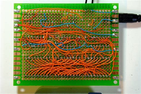
In through-hole assembly, components with long leads are inserted through holes drilled in the PCB and soldered to pads on the opposite side. This technique is suitable for larger components and provides strong mechanical connections, making it ideal for applications that require high reliability and durability.
2. Surface-Mount Assembly (SMA)
In surface-mount assembly, components with small leads or terminations are mounted directly onto pads on the surface of the PCB. This technique allows for higher component density, smaller board sizes, and faster assembly compared to through-hole assembly. Surface-mount assembly is widely used in modern electronic devices due to its space-saving and cost-effective nature.
PCB Testing and Inspection
To ensure the quality and reliability of the assembled circuit board, various testing and inspection techniques are employed. Some of the most common methods include:
1. Visual inspection
A visual inspection is performed to check for any obvious defects, such as missing or misaligned components, solder bridges, or damaged traces.
2. Automated Optical Inspection (AOI)
AOI uses high-resolution cameras and image processing software to automatically detect assembly defects, such as missing or misplaced components, solder joint issues, and trace defects.
3. X-ray inspection
X-ray inspection is used to examine solder joints and other internal structures that are not visible from the surface, particularly in multi-layer boards and ball grid array (BGA) packages.
4. In-Circuit Testing (ICT)
ICT involves using a bed-of-nails fixture to make electrical contact with specific points on the PCB and verifying the functionality of individual components and circuits.
5. Functional testing
Functional testing is performed to ensure that the assembled PCB meets its intended performance specifications and functions as expected in its final application.
Frequently Asked Questions (FAQ)
1. What is the difference between a schematic diagram and a PCB layout?
A schematic diagram represents the electrical connections between components using symbols and lines, while a PCB layout shows the physical placement and routing of components and traces on the actual circuit board.
2. Can a circuit board be repaired if damaged?
In some cases, a damaged circuit board can be repaired by replacing faulty components or repairing damaged traces. However, the feasibility and cost-effectiveness of the repair depend on the extent of the damage and the complexity of the board.
3. What is the purpose of a solder mask on a circuit board?
A solder mask is a protective layer applied to the surface of a circuit board that covers the copper traces while leaving the pads and holes exposed. It helps prevent short circuits, provides insulation, and protects the traces from damage during handling and assembly.
4. How do I choose the right type of circuit board for my project?
The choice of circuit board type depends on several factors, such as the complexity of the circuit, the required performance and reliability, the available space, and the budget. Consult with a PCB design professional or manufacturer to determine the most suitable type for your specific application.
5. What are the environmental concerns associated with circuit board manufacturing and disposal?
Circuit board manufacturing involves the use of hazardous chemicals and materials, which can pose environmental risks if not handled and disposed of properly. Additionally, electronic waste, including discarded circuit boards, can release toxic substances into the environment if not recycled or disposed of responsibly. Proper waste management and recycling practices are crucial to mitigating these environmental concerns.


Leave a Reply