Introduction to PCB Manufacturing
Printed Circuit Board (PCB) manufacturing is a critical process in the electronics industry, enabling the creation of complex circuitry on a compact and durable substrate. PCBs are found in nearly all electronic devices, from smartphones and computers to industrial equipment and medical devices. This article will provide an in-depth look at the PCB manufacturing process, covering everything from PCB design and material selection to the various manufacturing steps and quality control measures.
What is a Printed Circuit Board (PCB)?
A Printed Circuit Board (PCB) is a flat board made of insulating material, such as fiberglass or composite epoxy, with conductive copper traces printed onto its surface. These copper traces form the electrical connections between components mounted on the board, allowing for complex circuits to be created in a compact and organized manner.
PCBs come in various types, depending on the number of layers and the density of components:
| PCB Type | Description |
|---|---|
| Single-layer PCB | Has conductive traces on one side of the board only |
| Double-layer PCB | Has conductive traces on both sides of the board |
| Multi-layer PCB | Has multiple layers of conductive traces separated by insulating layers |
| High Density Interconnect (HDI) PCB | Has a higher density of components and finer trace widths and spacing |
Advantages of Using PCBs
Using PCBs in electronic devices offers several advantages over other methods of circuit construction, such as point-to-point wiring or wire wrapping:
- Compact size: PCBs allow for complex circuits to be created in a small space, enabling the miniaturization of electronic devices.
- Reliability: The solid substrate and precise manufacturing process make PCBs highly reliable, with fewer chances of short circuits or broken connections.
- Consistency: PCBs are manufactured using automated processes, ensuring consistent quality and reducing the risk of human error.
- Cost-effective: Mass production of PCBs is cost-effective, as the automated manufacturing process reduces labor costs and material waste.
PCB Design and Material Selection
PCB Design Software
Creating a PCB begins with the design phase, where the circuit schematic is translated into a physical layout. This is typically done using specialized PCB design software, such as Altium Designer, KiCad, or Eagle. These software packages allow designers to create schematic diagrams, define component footprints, and lay out the copper traces and drill holes on the board.
Material Selection
The choice of PCB substrate material depends on the specific requirements of the application, such as the operating temperature, frequency, and environmental conditions. Common PCB substrate materials include:
| Material | Description | Applications |
|---|---|---|
| FR-4 | A composite material made of fiberglass and epoxy resin | General-purpose PCBs |
| High Tg FR-4 | FR-4 with a higher glass transition temperature | High-temperature applications |
| Polyimide | A high-performance polymer with excellent thermal and chemical resistance | Aerospace and military applications |
| Teflon (PTFE) | A low-loss material with excellent high-frequency properties | RF and microwave applications |
The copper traces on the PCB are typically made of electrodeposited copper foil, which is laminated onto the substrate material. The thickness of the copper foil is specified in ounces per square foot (oz/ft²), with common thicknesses ranging from 0.5 oz/ft² to 2 oz/ft².

PCB Manufacturing Process
The PCB manufacturing process involves several steps, each of which must be carefully controlled to ensure the quality and reliability of the final product.
Step 1: PCB Design and Gerber File Generation
Once the PCB design is finalized, the design software generates a set of Gerber files, which are the industry-standard format for describing the layout of the PCB. The Gerber files contain information about the copper traces, drill holes, solder mask, and silkscreen layers of the PCB.
Step 2: PCB Fabrication
The actual manufacturing of the PCB begins with the fabrication of the bare board. This involves several sub-steps:
- Copper clad laminate: The substrate material is cut to size and laminated with copper foil on one or both sides.
- Drilling: Holes are drilled through the board to accommodate through-hole components and vias.
- Copper patterning: The unwanted copper is etched away, leaving only the desired traces and pads. This is typically done using a photolithography process, where a photoresist layer is applied, exposed to UV light through a photomask, and developed to create the desired pattern.
- Solder mask application: A layer of solder mask is applied to the board, covering the copper traces but leaving the pads exposed. This helps to prevent short circuits and provides insulation.
- Silkscreen printing: A silkscreen layer is printed onto the board, adding text and symbols for component identification and assembly instructions.
- Surface finish: A surface finish, such as HASL (Hot Air Solder Leveling), ENIG (Electroless Nickel Immersion Gold), or OSP (Organic Solderability Preservative), is applied to the exposed pads to improve solderability and protect against oxidation.
Step 3: PCB Assembly
After the bare board is fabricated, the components are mounted onto the board to complete the PCB assembly. This can be done using two main methods:
- Through-hole assembly: Components with wire leads are inserted through the drilled holes and soldered onto the pads on the opposite side of the board.
- Surface mount assembly: Components with flat terminations are placed directly onto the pads on the surface of the board and soldered in place.
The soldering process is typically done using one of two methods:
- Wave soldering: The board is passed over a wave of molten solder, which wicks up through the through-holes and solders the components in place.
- Reflow soldering: Solder paste is applied to the pads, the components are placed, and the board is heated in a reflow oven to melt the solder and form the connections.
Step 4: Quality Control and Testing
After the PCB assembly is complete, the board undergoes various quality control and testing procedures to ensure its functionality and reliability. These may include:
- Visual inspection: The board is visually inspected for any defects, such as missing components, solder bridges, or damaged traces.
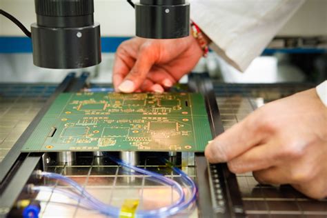
- Automated Optical Inspection (AOI): An automated camera system scans the board and compares it to the original design files, highlighting any discrepancies.
- X-ray inspection: X-ray imaging is used to inspect the solder joints and internal layers of the board for any defects or voids.
- Electrical testing: The board is powered up and its functionality is tested using specialized test equipment, such as in-circuit testers or Flying Probe Testers.
- Environmental testing: The board may be subjected to environmental stress tests, such as thermal cycling or vibration testing, to ensure its durability and reliability.

PCB Manufacturing Service Providers
Many companies specialize in providing PCB manufacturing services, offering a range of capabilities and expertise to meet the needs of different applications and industries.
Choosing a PCB Manufacturing Service Provider
When selecting a PCB manufacturing service provider, consider the following factors:
- Manufacturing capabilities: Ensure that the provider has the necessary equipment and expertise to manufacture your specific type of PCB, whether it is a simple single-layer board or a complex HDI design.
- Quality certifications: Look for providers with industry-recognized quality certifications, such as ISO 9001, AS9100, or IPC-A-610, which demonstrate their commitment to quality and adherence to established standards.
- Turnaround time: Consider the provider’s typical turnaround times and whether they can accommodate your project timeline.
- Cost: Compare the prices of different providers, but be cautious of sacrificing quality for cost savings.
- Customer support: Choose a provider with responsive and knowledgeable customer support, as this can be invaluable in case of any issues or questions during the manufacturing process.

Frequently Asked Questions (FAQ)
1. What is the difference between a PCB and a PCBA?
A PCB (Printed Circuit Board) is the bare board with copper traces and pads, while a PCBA (Printed Circuit Board Assembly) is the complete board with components mounted and soldered onto it.
2. How long does it take to manufacture a PCB?
The turnaround time for PCB manufacturing varies depending on the complexity of the design and the manufacturing capabilities of the service provider. Simple PCBs can be manufactured in as little as 24 hours, while complex designs may take several weeks.
3. What is the minimum order quantity (MOQ) for PCB manufacturing?
The minimum order quantity for PCB manufacturing varies among service providers. Some providers offer low-volume prototyping services with MOQs as low as one piece, while others may require a minimum order of 100 or more pieces for production runs.
4. Can I manufacture PCBs with different colors?
Yes, PCBs can be manufactured with different solder mask colors, such as green, blue, red, or black. Some service providers also offer custom silkscreen colors for logos or text.
5. What file formats are required for PCB manufacturing?
The most common file format for PCB manufacturing is the Gerber format, which includes separate files for each layer of the PCB (copper traces, solder mask, silkscreen, etc.). Other common file formats include ODB++, IPC-2581, and DXF.
Conclusion
PCB manufacturing is a complex process that involves multiple steps and requires specialized equipment and expertise. By understanding the basics of PCB design, material selection, and the manufacturing process, you can make informed decisions when choosing a PCB manufacturing service provider and ensure the success of your electronic projects.
As the electronics industry continues to evolve, PCB manufacturing technologies will advance to meet the demands for smaller, faster, and more reliable electronic devices. By staying up-to-date with the latest developments in PCB manufacturing and partnering with reputable service providers, you can stay ahead of the curve and bring your innovative ideas to life.


Leave a Reply