Introduction to PCB Optimization
Printed Circuit Board (PCB) optimization is a crucial aspect of electronic product design and manufacturing. It involves various techniques and strategies to enhance the performance, reliability, and cost-effectiveness of PCBs. One of the key factors in PCB optimization is panel utilization, which refers to the efficient use of the available space on a PCB panel to maximize the number of PCBs produced per panel.
Why is PCB Optimization Important?
PCB optimization is essential for several reasons:
- Cost reduction: Optimizing PCB design and panel utilization can significantly reduce manufacturing costs by minimizing material waste and increasing production efficiency.
- Improved performance: Optimized PCBs exhibit better electrical performance, reduced signal interference, and enhanced thermal management.
- Increased reliability: Properly optimized PCBs are less prone to defects and failures, resulting in higher product reliability and customer satisfaction.
- Faster time-to-market: Efficient PCB optimization streamlines the design and manufacturing process, enabling faster product development and shorter time-to-market.
Factors Affecting Panel Utilization
Several factors influence panel utilization in PCB manufacturing:
1. PCB Size and Shape
The size and shape of the individual PCBs play a significant role in panel utilization. Smaller PCBs allow for more units to be placed on a single panel, while larger or irregularly shaped PCBs may result in lower panel utilization.
2. Panelization Scheme
The panelization scheme refers to the arrangement of PCBs on the panel. There are various panelization techniques, such as:
- Grid panelization: PCBs are arranged in a regular grid pattern on the panel.
- Stepped panelization: PCBs are arranged in a staggered or stepped pattern to maximize panel utilization.
- Custom panelization: PCBs are arranged in a custom layout to accommodate specific design requirements or manufacturing constraints.
3. Manufacturing Constraints
Manufacturing constraints, such as minimum spacing between PCBs, edge clearance, and tooling requirements, impact panel utilization. These constraints ensure proper fabrication and assembly of the PCBs while maintaining the structural integrity of the panel.
4. Material Selection
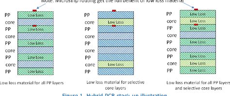
The choice of PCB material affects panel utilization. Some materials, such as high-frequency laminates or flexible substrates, may have specific manufacturing requirements that influence panel layout and utilization.
Strategies for Optimizing Panel Utilization
To optimize panel utilization and maximize the number of PCBs per panel, consider the following strategies:
1. PCB Design Optimization
- Minimize PCB size: Design PCBs with the smallest possible dimensions while ensuring functionality and manufacturability.
- Standardize PCB sizes: Use standard PCB sizes whenever possible to facilitate efficient panelization and reduce material waste.
- Optimize component placement: Place components strategically to minimize PCB size and improve routing efficiency.
2. Panelization Techniques
- Utilize stepped panelization: Arrange PCBs in a staggered or stepped pattern to maximize panel space utilization.
- Implement custom panelization: Develop custom panel layouts that accommodate specific design requirements or manufacturing constraints.
- Consider multi-array panelization: Combine multiple PCB designs on a single panel to optimize material usage and reduce setup times.
3. Manufacturing Process Optimization
- Collaborate with PCB manufacturers: Work closely with PCB manufacturers to understand their specific manufacturing capabilities and constraints.
- Optimize tooling and routing: Minimize the number of tooling holes and optimize routing paths to reduce material waste and improve manufacturing efficiency.
- Implement Design for Manufacturing (DFM) principles: Follow DFM guidelines to ensure PCB designs are compatible with manufacturing processes and minimize potential issues.
4. Material Selection and Inventory Management
- Choose materials wisely: Select PCB materials that balance performance requirements with manufacturing constraints and cost considerations.
- Optimize material inventory: Implement effective inventory management strategies to minimize material waste and optimize purchasing decisions.
- Consider material standardization: Standardize materials across multiple PCB designs to improve inventory management and reduce costs.

PCB Panel Utilization Metrics
To assess the effectiveness of panel utilization optimization efforts, consider the following metrics:
| Metric | Definition | Formula |
|---|---|---|
| Panel Utilization Ratio | The ratio of the total area of PCBs to the total panel area | (Total PCB Area) / (Total Panel Area) × 100% |
| PCBs per Panel | The number of PCBs that can be manufactured from a single panel | (Total Panel Area) / (Individual PCB Area) |
| Material Utilization Efficiency | The ratio of the total PCB area to the total material used | (Total PCB Area) / (Total Material Used) × 100% |
By tracking these metrics, you can quantify the impact of optimization strategies and identify areas for further improvement.
Best Practices for PCB Panel Optimization
To achieve optimal panel utilization, consider the following best practices:
- Collaborate with stakeholders: Engage with PCB designers, manufacturers, and other stakeholders to ensure a holistic approach to panel optimization.
- Conduct design reviews: Regularly review PCB designs to identify opportunities for optimization and ensure compliance with manufacturing constraints.
- Utilize simulation and modeling: Employ simulation and modeling tools to evaluate different panelization schemes and optimize panel layouts.
- Implement continuous improvement: Continuously monitor and analyze panel utilization metrics to identify areas for improvement and implement necessary changes.
- Stay updated with industry trends: Keep abreast of the latest advancements in PCB manufacturing technologies and materials to leverage new opportunities for optimization.
Frequently Asked Questions (FAQ)
1. What is the difference between panel utilization and material utilization?
Panel utilization focuses on maximizing the number of PCBs that can be manufactured from a single panel, while material utilization refers to the efficient use of PCB materials to minimize waste and costs.
2. How can I determine the optimal panelization scheme for my PCB design?
The optimal panelization scheme depends on various factors, such as PCB size, shape, manufacturing constraints, and production volume. Collaborate with your PCB manufacturer and utilize simulation and modeling tools to evaluate different panelization options and select the most suitable one for your specific requirements.
3. What are the benefits of standardizing PCB sizes?
Standardizing PCB sizes offers several benefits, including improved panel utilization, reduced material waste, simplified inventory management, and faster manufacturing setup times. It also facilitates the use of common tooling and processes, leading to cost savings and increased production efficiency.
4. How can I ensure my PCB design is compatible with manufacturing constraints?
To ensure PCB design compatibility with manufacturing constraints, follow Design for Manufacturing (DFM) guidelines provided by your PCB manufacturer. Regularly communicate with the manufacturing team to understand their specific requirements and constraints, and incorporate them into your design process. Conduct design reviews and utilize DFM analysis tools to identify and resolve potential manufacturability issues early in the design cycle.
5. What are the potential challenges in implementing panel utilization optimization strategies?
Implementing panel utilization optimization strategies may involve challenges such as balancing design requirements with manufacturing constraints, managing trade-offs between panel utilization and other design factors (e.g., signal integrity, thermal management), and ensuring effective communication and collaboration among stakeholders. Additionally, optimizing panel utilization may require investments in specialized software tools, training, and process improvements. However, the long-term benefits of improved efficiency, cost savings, and product quality often outweigh these challenges.
Conclusion
PCB Panel Size optimization is a critical aspect of PCB manufacturing that directly impacts production efficiency, cost, and product quality. By understanding the factors affecting panel utilization and implementing effective optimization strategies, you can maximize the number of PCBs produced per panel, reduce material waste, and improve overall manufacturing performance.
Key strategies for optimizing panel utilization include PCB design optimization, panelization techniques, manufacturing process optimization, and material selection and inventory management. By collaborating with stakeholders, conducting regular design reviews, utilizing simulation and modeling tools, and implementing continuous improvement practices, you can achieve significant improvements in panel utilization and drive success in your PCB manufacturing operations.
As the electronics industry continues to evolve, staying updated with the latest technologies, materials, and best practices in PCB optimization is crucial for maintaining a competitive edge. By embracing a proactive approach to panel utilization optimization, you can unlock new opportunities for cost savings, enhanced product quality, and faster time-to-market in the dynamic world of PCB manufacturing.
Leave a Reply