Why is PCB Testing Important?
PCB testing is vital for several reasons:
-
Quality Assurance: Testing helps ensure that the manufactured PCBs meet the required specifications and standards, guaranteeing a high-quality end product.
-
Reliability: Thorough testing identifies potential issues and defects, preventing premature failures and enhancing the overall reliability of the PCB.
-
Cost Savings: Detecting and fixing issues early in the manufacturing process reduces the cost of rework and prevents expensive product recalls.
-
Customer Satisfaction: By delivering fully functional and reliable PCBs, manufacturers can improve customer satisfaction and maintain a good reputation in the market.
The 8 Essential PCB Testing Methods
1. Visual Inspection
Visual inspection is the first line of defense in PCB testing. This method involves carefully examining the PCB for any visible defects or irregularities. Inspectors look for issues such as:
- Solder bridges or shorts
- Incorrect component placement
- Damaged or missing components
- Contamination or foreign objects
Visual inspection can be performed manually using magnifying lenses or microscopes or with the help of automated optical inspection (AOI) systems.
2. Automated Optical Inspection (AOI)
AOI is a more advanced form of visual inspection that uses high-resolution cameras and image processing software to detect defects on the PCB surface. AOI systems compare the captured images of the PCB with a pre-defined set of design rules and identify any discrepancies. Some advantages of AOI include:
- High-speed inspection
- Consistent and repeatable results
- Ability to detect small defects that may be missed by manual inspection
3. X-Ray Inspection
X-ray inspection is a non-destructive testing method that allows for the examination of internal structures and components of a PCB. This method is particularly useful for inspecting:
- Ball Grid Array (BGA) connections
- Flip-chip devices
- Vias and through-hole components
X-ray inspection systems use either 2D or 3D imaging techniques to create detailed images of the PCB’s internal structure, enabling the detection of hidden defects such as voids, cracks, or poor solder joints.
4. In-Circuit Testing (ICT)
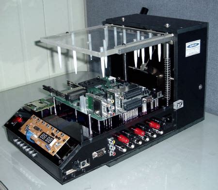
In-circuit testing is a method that verifies the functionality of individual components on the PCB by directly accessing their pins using a bed-of-nails fixture. ICT checks for:
- Short circuits
- Open circuits
- Resistance values
- Capacitance values
- Diode and transistor functionality
ICT is an efficient way to identify faulty components and ensure that they meet the specified tolerances.
5. Flying Probe Testing
Flying probe testing is an alternative to ICT that uses movable probes to access test points on the PCB. This method offers several advantages over traditional ICT:
- No need for custom bed-of-nails fixtures
- Ability to test high-density PCBs with limited access points
- Flexibility to accommodate design changes
Flying probe testing is slower than ICT but provides greater coverage and adaptability.
6. Functional Testing
Functional testing verifies that the assembled PCB performs as intended by simulating real-world operating conditions. This testing method typically involves:
- Powering up the PCB
- Applying test signals
- Monitoring outputs
- Checking for proper functionality
Functional testing ensures that the PCB meets the specified performance requirements and can withstand the expected operating conditions.
7. Boundary Scan Testing
Boundary scan testing, also known as JTAG (Joint Test Action Group) testing, is a method that uses built-in test circuitry to verify the connectivity and functionality of digital components on the PCB. This method involves:
- Accessing the boundary-scan architecture of the components
- Applying test patterns to the input pins
- Capturing the output responses
- Comparing the results with the expected values
Boundary scan testing is particularly useful for testing complex, high-density PCBs with limited physical access points.
8. Burn-In Testing
Burn-in testing is a method that subjects the PCB to elevated temperatures and operating conditions for an extended period to identify potential early-life failures. This testing helps to:
- Stress the components and connections
- Identify weak components that may fail prematurely
- Ensure the long-term reliability of the PCB
Burn-in testing is typically performed in specialized chambers that can control temperature, humidity, and other environmental factors.
Choosing the Right PCB Testing Methods
When selecting the appropriate PCB testing methods for your project, consider the following factors:
- PCB complexity and density
- Component types and packages
- Accessibility of test points
- Required test coverage and accuracy
- Production volume and testing speed
- Budget and resource constraints
In most cases, a combination of testing methods is necessary to ensure comprehensive coverage and the highest quality of the final product.

Frequently Asked Questions (FAQ)
-
Q: What is the difference between AOI and visual inspection?
A: AOI uses automated cameras and image processing software to detect defects, while visual inspection relies on human inspectors using magnifying lenses or microscopes. AOI is faster, more consistent, and can detect smaller defects compared to manual visual inspection. -
Q: Can X-ray inspection detect all types of defects?
A: X-ray inspection is particularly effective for detecting defects in hidden or internal structures, such as BGA connections and vias. However, it may not be suitable for detecting surface-level defects or issues with component functionality. -
Q: Is in-circuit testing necessary if flying probe testing is used?
A: In-circuit testing and flying probe testing serve similar purposes but have different advantages. Flying probe testing offers greater flexibility and coverage but is slower than ICT. The choice between the two methods depends on factors such as PCB complexity, test coverage requirements, and production volume. -
Q: How long does burn-in testing typically take?
A: The duration of burn-in testing depends on the specific requirements of the product and the industry standards. It can range from a few hours to several days or even weeks, depending on the expected lifecycle of the product and the desired level of reliability. -
Q: Can functional testing replace all other testing methods?
A: While functional testing is essential for verifying the overall performance of the PCB, it cannot replace other testing methods that focus on specific aspects, such as component-level functionality, connectivity, or physical defects. A comprehensive testing strategy should include a combination of methods to ensure the highest quality and reliability of the PCB.
Conclusion
PCB testing is a multi-faceted process that requires a range of methods to ensure the quality, reliability, and functionality of the final product. The eight essential testing methods discussed in this article – visual inspection, AOI, X-ray inspection, ICT, flying probe testing, functional testing, boundary scan testing, and burn-in testing – each have their own strengths and applications.
By understanding these testing methods and their respective advantages, PCB manufacturers can develop a comprehensive testing strategy tailored to their specific needs. Implementing a robust testing process not only guarantees the quality of the PCBs but also helps to reduce costs, improve customer satisfaction, and maintain a competitive edge in the market.
As PCB technology continues to evolve, staying up-to-date with the latest testing methods and best practices is crucial for success in the electronics industry. By investing in the right testing equipment, expertise, and processes, manufacturers can deliver high-quality, reliable PCBs that meet the ever-increasing demands of modern electronic devices.
Leave a Reply