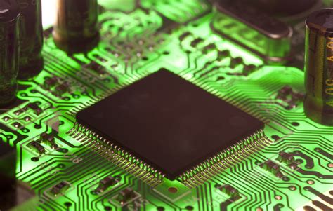
What is PCBA Manufacturing?
PCBA manufacturing is the process of assembling various electronic components onto a printed circuit board (PCB) to create a functional electronic device. The process involves several steps, including PCB design, component selection, solder paste application, component placement, reflow soldering, inspection, and testing.
The PCBA Manufacturing Process
Step 1: PCB Design
The first step in PCBA manufacturing is designing the printed circuit board. This involves creating a schematic diagram and a layout using specialized software such as Altium Designer, Eagle, or KiCad. The schematic diagram represents the electrical connections between components, while the layout determines the physical placement of components on the board.
PCB Design Considerations
When designing a PCB, several factors must be considered:
- Component selection and placement
- Signal integrity and electromagnetic compatibility
- Thermal management
- Manufacturing constraints (e.g., minimum trace width, hole size)
Step 2: PCB Fabrication
Once the PCB design is finalized, the next step is to fabricate the bare PCB. This process involves the following sub-steps:
-
Substrate preparation: The PCB substrate, typically made of FR-4 (a glass-reinforced epoxy laminate), is cut to the required size.
-
Copper cladding: A thin layer of copper is laminated onto the substrate.
-
Patterning: The desired circuit pattern is transferred onto the copper layer using photolithography.
-
Etching: Unwanted copper is removed using a chemical etching process, leaving only the desired circuit pattern.
-
Drilling: Holes are drilled into the PCB for through-hole components and vias.
-
Surface finish: A protective layer, such as HASL (Hot Air Solder Leveling) or ENIG (Electroless Nickel Immersion Gold), is applied to the exposed copper to prevent oxidation and improve solderability.
Step 3: Solder Paste Application
With the bare PCB ready, the next step is to apply solder paste to the pads where surface mount components will be placed. Solder paste is a mixture of tiny solder particles and flux, which helps to remove oxides and promote solder wetting during the reflow process.
Solder paste is typically applied using a stencil printing process:
- A stencil with openings corresponding to the component pads is aligned with the PCB.
- Solder paste is dispensed onto the stencil and spread using a squeegee.
- The stencil is removed, leaving precise deposits of solder paste on the pads.
Step 4: Component Placement
After solder paste application, surface mount components are placed onto the PCB using a pick-and-place machine. These machines use vacuum nozzles to pick up components from reels or trays and place them accurately on the solder paste deposits.
Component placement machines can be categorized based on their accuracy and speed:
| Machine Type | Accuracy | Speed (components per hour) |
|---|---|---|
| Entry-level | ±100 µm | Up to 5,000 |
| Mid-range | ±50 µm | 10,000 – 30,000 |
| High-end | ±20 µm | 50,000 – 100,000 |
Step 5: Reflow Soldering
Once all the components are placed, the PCB undergoes reflow soldering. In this process, the board is heated in a reflow oven, causing the solder paste to melt and form a permanent electrical and mechanical connection between the components and the PCB.
A typical reflow temperature profile consists of four stages:
- Preheat: The PCB is gradually heated to activate the flux and remove any moisture.
- Soak: The temperature is maintained to allow the components and board to reach a uniform temperature.
- Reflow: The temperature is quickly raised above the melting point of the solder, causing it to melt and wet the component leads and pads.
- Cooling: The PCB is cooled at a controlled rate to allow the solder joints to solidify without defects.
Step 6: Inspection and Testing
After reflow soldering, the assembled PCB undergoes various inspection and testing processes to ensure its quality and functionality:
- Visual inspection: The board is visually checked for defects such as bridging, tombstoning, or missing components.
- Automated Optical Inspection (AOI): An automated system captures images of the PCB and compares them to a reference to detect any defects.
- X-ray inspection: Used for detecting defects in hidden solder joints, such as those under Ball Grid Array (BGA) components.
- In-Circuit Testing (ICT): The board is placed in a bed-of-nails fixture that makes electrical contact with test points on the PCB, allowing for the verification of component values and Circuit Continuity.
- Functional testing: The assembled PCB is powered up and tested for its intended functionality using specialized test equipment or software.
Step 7: Final Assembly and Packaging
Once the PCBA has passed all inspections and tests, it may undergo final assembly, which can include:
- Mounting the PCBA into an enclosure or chassis
- Connecting any additional wiring or cables
- Installing any necessary mechanical components (e.g., buttons, connectors, or displays)
Finally, the completed product is packaged and ready for shipment to the customer.

Frequently Asked Questions (FAQ)
- What is the difference between PCB and PCBA?
-
A PCB is a bare printed circuit board without any components mounted on it, while a PCBA is a fully assembled board with components soldered onto it.
-
What are the most common PCB surface finishes?
-
The most common PCB surface finishes are HASL (Hot Air Solder Leveling), ENIG (Electroless Nickel Immersion Gold), and OSP (Organic Solderability Preservative).
-
What is the purpose of solder paste in PCBA manufacturing?
-
Solder paste serves two main purposes: it provides a mechanical and electrical connection between components and the PCB, and the flux in the paste helps to remove oxides and promote solder wetting during the reflow process.
-
What are some common defects that can occur during PCBA manufacturing?
-
Common defects include bridging (unintended connections between adjacent pads), tombstoning (components standing up on one end), solder balls, and insufficient or excessive solder.
-
What is the role of inspection and testing in PCBA manufacturing?
- Inspection and testing are critical for ensuring the quality and functionality of the assembled PCB. They help to identify and correct any defects or issues before the product is shipped to the customer, reducing the risk of field failures and returns.

Conclusion
PCBA manufacturing is a multi-step process that requires precision, skill, and advanced technology. By understanding the various stages involved, from PCB design to final assembly, you can better appreciate the complexity and importance of each step in creating a high-quality, functional electronic product.
As technology continues to advance, PCBA manufacturing processes will evolve to keep pace with the increasing demand for smaller, more complex, and higher-performance electronic devices. By staying informed about the latest developments in PCBA manufacturing, you can ensure that your products remain competitive in today’s rapidly changing market.


Leave a Reply