What is PCB Silkscreening?
PCB silkscreening, also known as legend printing, is the process of applying ink onto the surface of a printed circuit board (PCB) to create text, logos, and other identifying marks. This technique is widely used in the electronics industry to improve the readability, aesthetics, and overall functionality of PCBs.
Silkscreening on PCBs serves several purposes:
- Component identification
- Orientation and placement guides
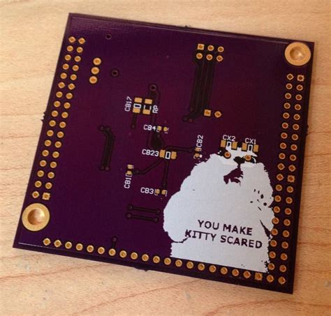
- Branding and logos
- Warnings and instructions
- Regulatory compliance marks
The Silkscreening Process
The PCB silkscreening process involves several steps:
-
Artwork Preparation: The desired artwork, including text and graphics, is created using CAD software. The artwork is then separated into individual layers for each color to be printed.
-
Screen Preparation: A fine mesh screen, typically made of polyester or stainless steel, is coated with a light-sensitive emulsion. The artwork is then exposed onto the screen, hardening the emulsion where the artwork is transparent.
-
Ink Application: The screen is placed over the PCB, and ink is applied using a squeegee. The ink passes through the open areas of the screen, transferring the artwork onto the PCB surface.
-
Curing: The printed ink is then cured using heat or UV light to ensure its durability and adherence to the PCB surface.
Advantages of PCB Silkscreening
PCB silkscreening offers several advantages over other marking methods:
-
Durability: Silkscreened marks are highly resistant to abrasion, chemicals, and extreme temperatures, ensuring long-lasting readability.
-
Precision: The fine mesh screens used in silkscreening allow for high-resolution printing, resulting in crisp, detailed marks.
-
Versatility: Silkscreening can be applied to various PCB Materials, including FR-4, aluminum, and flexible substrates.
-
Cost-effectiveness: For large-scale production, silkscreening is a cost-effective marking solution compared to other methods like laser etching or direct inkjet printing.

Considerations for PCB Silkscreening
When incorporating silkscreening into PCB design, several factors should be considered:
-
Ink Color: White ink is the most common choice for silkscreening, as it provides high contrast against the typical green solder mask. However, other colors can be used for specific applications or to match branding requirements.
-
Font Size and Style: The font size and style should be chosen to ensure readability while considering the available space on the PCB. A minimum font size of 0.8mm is recommended for legibility.
-
Placement: Silkscreened marks should be placed in areas that do not interfere with component placement or soldering. Adequate clearance should be maintained around pads and traces.
-
Design Rules: PCB Manufacturers often have specific design rules for silkscreening, such as minimum line width and spacing. Adhering to these rules ensures the best print quality and helps avoid manufacturing issues.

Alternatives to PCB Silkscreening
While silkscreening is the most common method for applying legends to PCBs, there are alternative techniques available:
-
Direct Inkjet Printing: This method uses specialized inkjet printers to apply marks directly onto the PCB surface. It offers greater flexibility in terms of customization and eliminates the need for screens, but it may be less durable than silkscreening.
-
Laser Etching: Laser etching uses a high-powered laser to remove the solder mask or substrate material, creating permanent marks on the PCB. This method is highly durable but may be more expensive and time-consuming than silkscreening.
-
Labeling: Pre-printed labels can be applied to the PCB surface as an alternative to direct printing. Labels offer flexibility and can be easily replaced if needed, but they may not be as durable as silkscreened or etched marks.

Frequently Asked Questions (FAQ)
1. How long does PCB silkscreening last?
Silkscreened marks on PCBs are highly durable and can last for the entire lifespan of the board if properly applied and cured. The ink is resistant to abrasion, chemicals, and extreme temperatures, ensuring long-lasting readability.
2. Can silkscreening be applied to both sides of a PCB?
Yes, silkscreening can be applied to both the top and bottom sides of a PCB. However, it is more common to have silkscreening on the top side, where components are typically placed.
3. What is the minimum font size for PCB silkscreening?
A minimum font size of 0.8mm is recommended for legibility in PCB silkscreening. However, the actual minimum size may vary depending on the specific PCB manufacturer and their capabilities.
4. Can silkscreening be used on Flexible PCBs?
Yes, silkscreening can be applied to flexible PCBs, but the process may require specialized inks and curing methods to ensure proper adhesion and flexibility.
5. Is it possible to have multiple colors in PCB silkscreening?
Yes, multiple colors can be used in PCB silkscreening. Each color requires a separate screen and printing pass, which may increase the cost and production time compared to single-color silkscreening.
Conclusion
PCB silkscreening is a versatile and essential technique for applying text, logos, and other identifying marks to printed circuit boards. Its durability, precision, and cost-effectiveness make it the preferred choice for many electronics manufacturers. By understanding the silkscreening process, its advantages, and design considerations, PCB designers can effectively incorporate this technique into their projects, enhancing the functionality and aesthetics of their boards.
As the electronics industry continues to evolve, PCB silkscreening remains a vital tool for ensuring the readability, branding, and overall quality of printed circuit boards. Whether used for component identification, orientation guides, or regulatory compliance, silkscreening plays a crucial role in the production of reliable and user-friendly electronic devices.


Leave a Reply