Introduction to PCB Thickness and Pin Length
In the world of printed circuit board (PCB) design, the thickness of the board and the length of the through hole pins are critical factors that determine the functionality, durability, and overall performance of the electronic device. The relationship between PCB thickness and pin length is a crucial aspect of the design process, as it affects the mechanical stability, electrical connectivity, and manufacturing feasibility of the PCB Assembly.
What is PCB Thickness?
PCB thickness refers to the distance between the top and bottom surfaces of the printed circuit board. It is typically measured in millimeters (mm) or thousandths of an inch (mil). The thickness of a PCB is determined by the number of layers it contains, the materials used, and the specific requirements of the application.
Common PCB thicknesses include:
| PCB Thickness (mm) | PCB Thickness (mil) |
|---|---|
| 0.4 | 15.75 |
| 0.6 | 23.62 |
| 0.8 | 31.50 |
| 1.0 | 39.37 |
| 1.2 | 47.24 |
| 1.6 | 62.99 |
What is Through Hole Pin Length?
Through hole pin length refers to the length of the metal pins that protrude from the bottom of a through hole component, such as a connector or a power module. These pins are inserted into the corresponding holes on the PCB and soldered to create a strong mechanical and electrical connection.
The pin length is measured from the bottom surface of the component to the tip of the pin. It is essential to choose the appropriate pin length based on the thickness of the PCB to ensure proper assembly and performance.
Factors Affecting PCB Thickness Choice
When deciding on the appropriate PCB thickness for a particular application, several factors must be considered:
1. Number of Layers
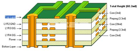
The number of layers in a PCB directly influences its thickness. As the number of layers increases, so does the thickness of the board. This is because each layer consists of a conductive copper foil laminated onto an insulating substrate material, which adds to the overall thickness.
| Number of Layers | Typical PCB Thickness (mm) |
|---|---|
| 1 | 0.4 – 0.6 |
| 2 | 0.6 – 0.8 |
| 4 | 1.0 – 1.2 |
| 6 | 1.2 – 1.6 |
| 8 | 1.6 – 2.0 |
2. Material Selection
The choice of materials used in the construction of a PCB also affects its thickness. The most common substrate material is FR-4, a glass-reinforced epoxy laminate. However, other materials such as polyimide, PTFE, or metal-Core substrates may be used for specific applications, which can result in different thicknesses.
3. Application Requirements
The specific requirements of the application play a significant role in determining the appropriate PCB thickness. For example, high-power applications may require thicker boards to dissipate heat effectively, while high-frequency applications may benefit from thinner boards to minimize signal loss and distortion.
Other application-specific factors that influence PCB thickness include:
- Mechanical stress and vibration
- Environmental conditions (temperature, humidity)
- Space constraints
- Weight restrictions

Factors Affecting Through Hole Pin Length Choice
Choosing the appropriate through hole pin length is crucial for ensuring proper assembly and performance of the PCB. The following factors should be considered when selecting pin length:
1. PCB Thickness
The thickness of the PCB is the primary factor in determining the appropriate pin length. The pin must be long enough to protrude through the board and allow for sufficient solder fillets on the bottom side. However, if the pin is too long, it may cause difficulties in assembly or pose a risk of damage during handling.
A general rule of thumb is to select a pin length that is at least 2-3 mm longer than the PCB thickness. This allows for adequate protrusion and soldering while minimizing the risk of excessive pin length.
| PCB Thickness (mm) | Recommended Pin Length (mm) |
|---|---|
| 0.4 | 2.4 – 3.4 |
| 0.6 | 2.6 – 3.6 |
| 0.8 | 2.8 – 3.8 |
| 1.0 | 3.0 – 4.0 |
| 1.2 | 3.2 – 4.2 |
| 1.6 | 3.6 – 4.6 |
2. Component Placement
The placement of through hole components on the PCB can also influence the choice of pin length. If components are placed close to the edge of the board, shorter pins may be necessary to avoid overhang and potential damage during handling or assembly.
Additionally, if components are placed on both sides of the board, the pin length must be carefully selected to ensure proper protrusion and soldering on both sides without causing interference or damage.
3. Manufacturing Considerations
The manufacturing process and equipment used for PCB assembly can also impact the choice of pin length. Some factors to consider include:
- Soldering method (wave, selective, hand)
- Solder paste application method (stencil, dispensing)
- Clearance requirements for automated assembly equipment
Consulting with the PCB manufacturer and assembly provider can help ensure that the selected pin length is compatible with their processes and equipment.

PCB Design Considerations for Optimal Pin Length
To ensure optimal performance and manufacturability, PCB designers should follow best practices when selecting pin lengths and designing through hole components:
1. Standardization
Whenever possible, use standardized pin lengths for through hole components. This simplifies the procurement process, reduces the risk of assembly errors, and improves overall manufacturability.
2. Tolerances
Consider the tolerances of both the PCB thickness and the pin length when designing the board. Ensure that the selected pin length allows for sufficient tolerance to accommodate variations in PCB thickness and pin length without compromising assembly or performance.
3. Solder Fillets
Design the PCB Layout to allow for adequate solder fillets on both sides of the through hole component. This ensures a strong mechanical and electrical connection and reduces the risk of solder joint failures.
4. Thermal Management
For high-power applications, consider using longer pins or thermal vias to improve heat dissipation. Longer pins provide a larger surface area for heat transfer, while thermal vias can conduct heat away from the component and into the PCB substrate.

Frequently Asked Questions (FAQ)
1. What happens if the through hole pin is too short for the PCB thickness?
If the pin is too short, it may not protrude sufficiently through the PCB, resulting in weak or incomplete solder joints. This can lead to poor electrical connectivity, mechanical instability, and potential reliability issues.
2. Can I use different pin lengths for the same component on a PCB?
While it is technically possible to use different pin lengths for the same component, it is generally not recommended. Using consistent pin lengths simplifies the assembly process, reduces the risk of errors, and improves overall manufacturability.
3. How do I determine the appropriate pin length for a custom PCB thickness?
To determine the appropriate pin length for a custom PCB thickness, follow the general rule of thumb: select a pin length that is 2-3 mm longer than the PCB thickness. For example, if your custom PCB is 1.4 mm thick, choose a pin length between 3.4 mm and 4.4 mm.
4. Can I modify the pin length of a through hole component?
In most cases, modifying the pin length of a through hole component is not recommended. Attempting to cut or extend the pins can damage the component, alter its electrical characteristics, and void any manufacturer warranties. If a specific pin length is required, it is best to source a component with the appropriate pin length from the manufacturer.
5. How does pin length affect the assembly process?
Pin length can affect the assembly process in several ways. If the pins are too long, they may interfere with other components or be difficult to insert into the PCB. If the pins are too short, they may not protrude sufficiently for proper soldering. Additionally, inconsistent pin lengths can cause issues with automated assembly equipment, leading to misalignment or incomplete solder joints.
Conclusion
The relationship between through hole pin length and PCB thickness is a critical aspect of PCB design and assembly. Choosing the appropriate pin length based on the PCB thickness ensures proper mechanical stability, electrical connectivity, and manufacturability.
By considering factors such as the number of layers, material selection, application requirements, component placement, and manufacturing considerations, PCB designers can optimize their designs for optimal performance and reliability.
Following best practices such as standardization, tolerance management, solder fillet design, and thermal management can further enhance the quality and manufacturability of through hole PCB assemblies.
As PCB technology continues to evolve, understanding the importance of pin length and PCB thickness will remain crucial for designing and manufacturing high-quality, reliable electronic devices.


Leave a Reply