Introduction to PCB Layout
Printed Circuit Board (PCB) layout is a crucial step in the electronic product development process. It involves the arrangement and interconnection of electronic components on a PCB to ensure optimal performance, reliability, and manufacturability. A well-designed PCB layout can significantly enhance the functionality and longevity of an electronic device, while a poorly designed layout can lead to signal integrity issues, electromagnetic interference (EMI), and manufacturing problems.
In this article, we will explore the various aspects of PCB layout design services, including the design process, best practices, and the benefits of outsourcing PCB layout to professional service providers.
The PCB Layout Design Process
1. Schematic Design
The PCB layout process begins with the creation of a schematic diagram. The schematic represents the logical connections between electronic components and serves as a blueprint for the PCB layout. It is essential to ensure that the schematic is accurate and complete before proceeding with the layout design.
2. Component Placement
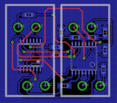
Once the schematic is finalized, the next step is to place the components on the PCB. The placement of components is critical to the overall performance and manufacturability of the PCB. Factors such as signal integrity, power distribution, thermal management, and mechanical constraints must be considered during component placement.
Best practices for component placement include:
- Grouping related components together
- Minimizing the distance between connected components
- Placing sensitive components away from sources of EMI
- Considering the orientation of components for optimal signal routing
- Ensuring adequate clearance between components for manufacturing and assembly
3. Signal Routing
Signal routing involves creating the copper traces that interconnect the components on the PCB. The goal of signal routing is to ensure that signals are transmitted efficiently and with minimal distortion. Factors such as trace width, spacing, and length must be carefully considered to maintain signal integrity.
Best practices for signal routing include:
- Using appropriate trace widths based on the current carrying requirements
- Maintaining consistent trace impedance throughout the signal path
- Avoiding sharp corners and using smooth curves for trace routing
- Minimizing the length of high-speed signal traces
- Separating sensitive signals from potential sources of interference
4. Power and Ground Planes
Power and ground planes are essential for distributing power and providing a stable reference voltage throughout the PCB. Proper design of power and ground planes can help minimize EMI and ensure reliable operation of the electronic device.
Best practices for power and ground plane design include:
- Using dedicated power and ground planes for each voltage level
- Providing adequate copper pour for power and ground planes
- Placing decoupling capacitors close to the power pins of components
- Using via stitching to connect power and ground planes across layers
- Avoiding split power and ground planes whenever possible
5. Design Rule Check (DRC)
Before finalizing the PCB layout, it is crucial to perform a Design Rule Check (DRC). The DRC ensures that the layout adheres to the manufacturing guidelines and constraints specified by the PCB fabricator. This includes checks for minimum trace widths, spacing, drill sizes, and other manufacturing parameters.
6. Output Files Generation
Once the PCB layout is complete and has passed the DRC, the final step is to generate the output files required for manufacturing. These files typically include:
- Gerber files: These are the industry-standard files used for PCB fabrication. They contain information about the copper layers, solder mask, silkscreen, and drill holes.
- Drill files: These files specify the location, size, and type of drill holes required for the PCB.
- Bill of Materials (BOM): The BOM lists all the components used in the PCB, along with their quantities and part numbers.
- Assembly drawings: These drawings provide instructions for the assembly of components on the PCB.

Benefits of Outsourcing PCB Layout Design
Outsourcing PCB layout design to professional service providers offers several benefits for electronic product development companies. Some of these benefits include:
- Expertise and Experience
Professional PCB layout designers have the expertise and experience necessary to create high-quality layouts that meet the specific requirements of each project. They are well-versed in industry standards, best practices, and the latest design tools and technologies.
- Time and Cost Savings
Outsourcing PCB layout design can help companies save time and reduce costs associated with maintaining an in-house design team. By leveraging the skills and resources of a professional service provider, companies can focus on their core competencies and bring products to market faster.
- Access to Advanced Tools and Technologies
PCB layout service providers invest in state-of-the-art design tools and technologies to ensure the highest quality layouts. These tools include advanced PCB design software, simulation tools, and automated design rule checking systems.
- Scalability and Flexibility
Outsourcing PCB layout design provides companies with the flexibility to scale their design capabilities up or down based on project demands. This allows companies to handle fluctuations in design workload without the need to hire additional in-house staff.
- Improved Design Quality
Professional PCB layout service providers have established quality control processes and methodologies to ensure that each layout meets the highest standards of quality and reliability. This can help reduce the risk of design errors and manufacturing issues, ultimately leading to better product performance and customer satisfaction.

Choosing the Right PCB Layout Design Service Provider
When selecting a PCB layout design service provider, it is essential to consider several factors to ensure a successful partnership. These factors include:
- Technical Expertise
Ensure that the service provider has the necessary technical expertise and experience in PCB layout design. Look for providers with a proven track record of delivering high-quality layouts for projects similar to yours.
- Communication and Collaboration
Effective communication and collaboration are critical to the success of any PCB layout project. Choose a service provider that values open communication and is willing to work closely with your team to understand your specific requirements and design goals.
- Design Tools and Technologies
Verify that the service provider uses industry-standard design tools and technologies to ensure compatibility with your existing design environment and manufacturing processes.
- Quality Assurance and Control
Inquire about the service provider’s quality assurance and control processes to ensure that the layouts meet your quality standards and are free from design errors.
- Cost and Delivery Time
Consider the cost and delivery time of the PCB layout design service in relation to your project budget and timeline. While cost is an important factor, it should not be the sole determining factor when choosing a service provider.

PCB Layout Design Best Practices
To ensure optimal performance and manufacturability of PCBs, it is essential to follow best practices in PCB layout design. Some of these best practices include:
-
Component Placement
-
Group related components together to minimize signal path lengths and reduce EMI.
- Place sensitive components away from sources of interference, such as power supplies and high-speed digital circuits.
-
Consider the orientation of components for optimal signal routing and thermal management.
-
Signal Routing
-
Use appropriate trace widths based on the current carrying requirements and signal frequency.
- Maintain consistent trace impedance throughout the signal path to minimize reflections and signal distortion.
- Avoid sharp corners and use smooth curves for trace routing to reduce signal reflections.
- Minimize the length of high-speed signal traces to reduce signal propagation delay and attenuation.
-
Separate sensitive signals from potential sources of interference using guard traces or shielding.
-
Power and Ground Planes
-
Use dedicated power and ground planes for each voltage level to provide a low-impedance power distribution network.
- Provide adequate copper pour for power and ground planes to minimize voltage drops and ensure stable reference voltages.
- Place decoupling capacitors close to the power pins of components to reduce power supply noise and improve signal integrity.
-
Use via stitching to connect power and ground planes across layers and minimize impedance discontinuities.
-
EMI and Signal Integrity
-
Minimize the loop area of high-speed signals to reduce EMI and crosstalk.
- Use ground planes to provide shielding and reduce EMI.
- Route high-speed signals on inner layers sandwiched between power and ground planes to minimize crosstalk and EMI.
-
Use differential signaling for high-speed signals to reduce EMI and improve signal integrity.
-
Manufacturing Considerations
-
Adhere to the manufacturing guidelines and constraints specified by the PCB fabricator, including minimum trace widths, spacing, drill sizes, and other parameters.
- Use standard component packages and footprints whenever possible to reduce manufacturing costs and lead times.
- Provide clear and concise assembly drawings and documentation to ensure accurate assembly of components on the PCB.
Common PCB Layout Design Challenges and Solutions
PCB layout designers often face various challenges that can impact the performance and manufacturability of PCBs. Some common challenges and their solutions include:
- High-Speed Signal Integrity
Challenge: High-speed signals are susceptible to signal integrity issues, such as reflections, crosstalk, and EMI.
Solution: Use appropriate trace routing techniques, such as controlled impedance traces, differential signaling, and proper termination. Minimize trace lengths and avoid sharp corners. Use ground planes for shielding and route high-speed signals on inner layers.
- Power Distribution
Challenge: Inadequate power distribution can lead to voltage drops, noise, and signal integrity issues.
Solution: Use dedicated power and ground planes with adequate copper pour. Place decoupling capacitors close to the power pins of components. Use via stitching to connect power and ground planes across layers.
- Thermal Management
Challenge: High-power components can generate excessive heat, leading to performance degradation and reliability issues.
Solution: Place high-power components away from sensitive components. Use thermal vias to transfer heat from components to the PCB’s copper layers. Consider using heatsinks or other thermal management techniques for critical components.
- Manufacturing Constraints
Challenge: PCB layouts must adhere to manufacturing constraints to ensure manufacturability and reduce costs.
Solution: Familiarize yourself with the manufacturing guidelines and constraints specified by the PCB fabricator. Use standard component packages and footprints whenever possible. Perform Design Rule Checks (DRC) to ensure compliance with manufacturing constraints.
- Electromagnetic Compatibility (EMC)
Challenge: PCBs must meet EMC requirements to ensure they do not interfere with other electronic devices and are not susceptible to external interference.
Solution: Follow EMC design guidelines, such as minimizing loop areas, using ground planes for shielding, and separating sensitive signals from potential sources of interference. Consider using filtering and shielding techniques to reduce EMI.
PCB Layout Design Tools and Software
There are several PCB layout design tools and software available in the market, ranging from entry-level to advanced professional-grade solutions. Some popular PCB layout design tools include:
- Altium Designer
Altium Designer is a comprehensive PCB design software that offers a wide range of features and capabilities, including schematic capture, 3D PCB layout, signal integrity analysis, and design rule checking.
- Cadence Allegro PCB Designer
Cadence Allegro PCB Designer is a powerful PCB layout design tool that provides advanced routing, placement, and analysis capabilities. It is widely used in the industry for designing complex, high-speed PCBs.
- Mentor Graphics PADS
Mentor Graphics PADS is a PCB design software suite that includes schematic capture, PCB layout, and analysis tools. It offers a user-friendly interface and is suitable for both entry-level and experienced PCB designers.
- KiCad
KiCad is a free and open-source PCB design software that offers schematic capture, PCB layout, and 3D viewing capabilities. It is a popular choice among hobbyists and small businesses.
- Eagle
Eagle is a widely used PCB design software that offers schematic capture, PCB layout, and autorouting capabilities. It is known for its ease of use and extensive component libraries.
When selecting a PCB layout design tool, consider factors such as ease of use, feature set, compatibility with your existing design environment, and cost. Many PCB layout design service providers use industry-standard tools to ensure compatibility and seamless collaboration with their clients.
Conclusion
PCB layout design is a critical aspect of electronic product development that directly impacts the performance, reliability, and manufacturability of PCBs. Outsourcing PCB layout design to professional service providers can offer numerous benefits, including access to expertise and experience, time and cost savings, and improved design quality.
To ensure successful PCB layout design, it is essential to follow best practices, such as proper component placement, signal routing, power and ground plane design, and adherence to manufacturing constraints. By working closely with experienced PCB layout designers and using industry-standard tools and technologies, companies can develop high-quality PCBs that meet their specific requirements and exceed customer expectations.
Frequently Asked Questions (FAQ)
-
What is PCB layout design?
PCB layout design is the process of arranging and interconnecting electronic components on a Printed Circuit Board (PCB) to ensure optimal performance, reliability, and manufacturability. -
Why is PCB layout design important?
PCB layout design is important because it directly impacts the functionality, reliability, and manufacturability of electronic devices. A well-designed PCB layout can enhance signal integrity, reduce electromagnetic interference (EMI), and minimize manufacturing issues. -
What are the benefits of outsourcing PCB layout design?
Outsourcing PCB layout design offers several benefits, including access to expertise and experience, time and cost savings, access to advanced tools and technologies, scalability and flexibility, and improved design quality. -
What factors should be considered when selecting a PCB layout design service provider?
When selecting a PCB layout design service provider, consider factors such as technical expertise, communication and collaboration, design tools and technologies, quality assurance and control, and cost and delivery time. -
What are some common PCB layout design challenges and solutions?
Common PCB layout design challenges include high-speed signal integrity, power distribution, thermal management, manufacturing constraints, and electromagnetic compatibility (EMC). Solutions to these challenges involve following best practices in component placement, signal routing, power and ground plane design, and adherence to manufacturing guidelines and EMC design principles.
| PCB Layout Design Best Practices | Description |
|---|---|
| Component Placement | – Group related components together – Place sensitive components away from sources of interference – Consider component orientation for optimal signal routing and thermal management |
| Signal Routing | – Use appropriate trace widths based on current and frequency requirements – Maintain consistent trace impedance – Avoid sharp corners and use smooth curves – Minimize high-speed signal trace lengths – Separate sensitive signals from potential sources of interference |
| Power and Ground Planes | – Use dedicated power and ground planes for each voltage level – Provide adequate copper pour – Place decoupling capacitors close to component power pins – Use via stitching to connect planes across layers |
| EMI and Signal Integrity | – Minimize loop area of high-speed signals – Use ground planes for shielding – Route high-speed signals on inner layers between power and ground planes – Use differential signaling for high-speed signals |
| Manufacturing Considerations | – Adhere to manufacturing guidelines and constraints – Use standard component packages and footprints when possible – Provide clear assembly drawings and documentation |


Leave a Reply