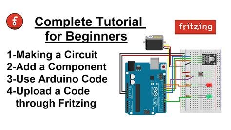
What is Fritzing and Why Use It for PCB Design?
Fritzing is an open-source software tool that allows users to easily design and create printed circuit boards (PCBs). It provides a user-friendly interface for designing electronic circuits, from simple breadboard layouts to complex PCBs ready for production. Some key features and benefits of using Fritzing for PCB design include:
| Feature | Benefit |
|---|---|
| Breadboard, schematic, and PCB views | Visualize circuits at different stages of the design process |
| Extensive part libraries | Quickly add common electronic components to designs |
| Arduino support | Easily integrate with Arduino boards and sketches |
| Autorouting | Automatically generate trace routing between components |
| Gerber file export | Produce industry-standard files for PCB fabrication |
Fritzing is ideal for hobbyists, students, and educators who want an accessible and intuitive tool for designing and prototyping electronic projects. Its visual interface and part libraries allow users to focus on the creative aspects of circuit design without getting bogged down in complex PCB layout tools.
Getting Started with Fritzing
To start using Fritzing for PCB design, follow these steps:
- Download and install Fritzing from the official website (https://fritzing.org/)
- Launch Fritzing and familiarize yourself with the interface
- Explore the part libraries and core concepts (breadboard, schematic, PCB views)
- Begin a new project by selecting your target Arduino board or creating a custom design
- Use the breadboard view to prototype your circuit and ensure proper connections
- Switch to schematic view to create a logical circuit diagram
- Transfer your schematic to the PCB view for physical board layout
- Utilize autorouting and manual adjustments to optimize component placement and routing
- Add custom art, text, and shapes to personalize your PCB design
- Export Gerber files and send them to a PCB fabrication service or produce your own boards
By following these steps, you’ll be able to quickly start designing functional and visually appealing PCBs in Fritzing. The key is to leverage the tool’s intuitive interface and features while adhering to best practices for circuit design and board layout.

Tips and Tricks for PCB Design in Fritzing
To get the most out of Fritzing and create high-quality PCBs, consider these tips and techniques:
Use a Consistent Grid and Spacing
When placing components and routing traces on your PCB, it’s important to use a consistent grid and maintain adequate spacing. This helps ensure proper manufacturing tolerances and reduces the risk of short circuits or interference. Fritzing allows you to set a custom grid size and snap components to the grid for precise placement.
Keep Trace Widths Appropriate for Current
The width of PCB traces should be selected based on the amount of current they need to carry. Thinner traces are prone to overheating and damage with high currents. Fritzing provides a trace width setting that can be adjusted based on your design requirements. Refer to standard trace width calculators or guidelines to determine the appropriate width for your expected current loads.
Minimize Trace Lengths and Crossovers
Long meandering traces and numerous intersections can degrade signal integrity and increase electromagnetic interference (EMI) in your PCB design. Try to minimize overall trace lengths by strategically placing components and choosing direct routing paths. Where trace crossovers are unavoidable, consider adding a via to route one trace to another layer, maintaining separation between signals.
Use Copper Pours for Shielding and Heat Dissipation
Copper pours, also known as ground planes or fills, are large areas of exposed copper on a PCB layer connected to ground. They provide several benefits such as reducing EMI, improving heat dissipation, and simplifying routing. In Fritzing, you can create copper pours by adding rectangular shapes on the copper layer and assigning them to the ground signal.
Label Key Components and Test Points
To aid in assembly, debugging, and maintenance of your PCB, it’s good practice to label important components, connectors, and test points. Fritzing allows you to easily add text labels on the silkscreen layer of your PCB design. Use descriptive labels and consider the text size for readability.
Verify Your Design Before Finalizing
Before exporting your PCB design for fabrication, thoroughly review and verify all aspects of your layout. Check for any missing connections, unrouted traces, or design rule violations. The Fritzing Design Rules Check (DRC) feature can help automate some of this verification. Carefully inspect your design in the PCB view, zooming in to check fine details and catching any errors before committing to production.
By applying these tips and continually refining your PCB design skills in Fritzing, you’ll be able to create functional, reliable, and professional-quality boards for your projects.

Advanced Fritzing Techniques for PCB Design
Once you’ve mastered the basics of PCB design in Fritzing, you can explore more advanced techniques to take your skills to the next level. Here are a few areas to focus on:
Custom Parts Creation
While Fritzing includes an extensive library of common electronic components, you may encounter projects that require custom or specialized parts. Fritzing allows you to create your own custom parts by defining their breadboard, schematic, and PCB representations. This involves creating vector graphics for each view and specifying pin mappings and metadata. Custom parts can then be saved and shared with the Fritzing community.
Multi-Layer PCB Design
Complex PCB designs often require the use of multiple copper layers to accommodate all the necessary traces and components. Fritzing supports up to four layers (top, bottom, and two inner layers) for PCB design. When working with multi-layer boards, it’s important to carefully plan your layer stackup and follow best practices for via placement and signal routing. Fritzing’s layer controls allow you to easily navigate and assign traces to different layers.
Panelization for Batch Production
If you plan to produce multiple copies of your PCB design, you can save time and cost by panelizing your boards. Panelization involves arranging multiple instances of your PCB design on a single larger board for fabrication. Fritzing does not have built-in panelization tools, but you can manually arrange copies of your design on a larger board outline and add alignment marks and breakaway tabs for easy separation after manufacturing.
Integrating External PCB Fabrication Services
While Fritzing can export industry-standard Gerber files for PCB fabrication, you may want to use external services that offer additional features or capabilities. Many PCB fabrication houses provide their own design rules and specifications that can be integrated into your Fritzing workflow. This may involve customizing drill sizes, trace widths, and clearances to match the fabricator’s requirements. Some services even offer direct integration with Fritzing through plugins or export scripts.
By exploring these advanced techniques, you can take your PCB designs to the next level and tackle more complex projects with confidence. Keep in mind that mastering PCB design is an iterative process that requires practice, experimentation, and continuous learning.

Frequently Asked Questions (FAQ)
- What is the maximum PCB size I can design in Fritzing?
Fritzing itself does not impose a hard limit on PCB size, but your design will be constrained by the capabilities of your chosen fabrication method. Most hobby-level PCB fabrication services have maximum size limits ranging from 10x10cm to 20x20cm. If you need larger boards, you may need to use more advanced design tools and fabrication processes.
- Can I import existing PCB designs into Fritzing?
Yes, Fritzing can import PCB designs from Eagle and KiCad file formats. To import an existing design, go to File > Open and select the appropriate file type. Keep in mind that some design elements or libraries may not translate perfectly between different tools, so you may need to make manual adjustments after importing.
- How do I create custom footprints for components in Fritzing?
To create a custom footprint in Fritzing, you’ll need to define the component’s breadboard, schematic, and PCB representations using SVG graphics. Start by creating a new part in the Parts Editor and specifying its properties and pin mappings. Then, use a vector graphics editor to create the visual representations for each view, following Fritzing’s SVG formatting guidelines. Once your custom part is complete, you can save it and use it in your PCB designs.
- What are the limitations of autorouting in Fritzing?
While Fritzing’s autorouting feature can save time and effort in PCB layout, it has some limitations compared to more advanced routing tools. Autorouting may not always find the most optimal path for traces, especially in dense or complex designs. It can also struggle with multi-layer routing and may not adhere to all design rules by default. For best results, use autorouting as a starting point and be prepared to make manual adjustments and optimizations.
- Can I use Fritzing for commercial PCB design projects?
Yes, Fritzing is released under the GNU GPL license, which allows for both personal and commercial use. However, it’s important to consider the limitations and capabilities of Fritzing compared to professional-grade PCB design tools. For complex, high-volume, or mission-critical commercial projects, you may want to use more advanced tools with features like simulation, signal integrity analysis, and design rule checking. Fritzing is best suited for hobbyist, educational, and prototyping applications.
By understanding the answers to these frequently asked questions, you’ll be better prepared to use Fritzing effectively and troubleshoot common issues that may arise in your PCB design process. Remember, the key to success with Fritzing is a combination of creativity, technical understanding, and a willingness to experiment and learn from your design experiences.


Leave a Reply