Introduction to PCB Fabrication
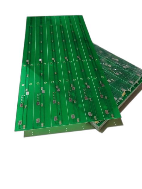
Printed Circuit Board (PCB) fabrication is the process of creating a functional circuit board from a design layout. PCBs are essential components in modern electronic devices, providing a platform for mounting and interconnecting electronic components. Two-layer PCBs are the most basic and commonly used type of PCB, consisting of two conductive layers separated by an insulating substrate.
In this article, we will delve into the process of two-layer PCB fabrication, covering the various steps involved, materials used, and best practices for ensuring high-quality PCBs.
Table of Contents
- PCB Design and Layout
- PCB Fabrication Materials
- PCB Fabrication Process
- Copper Clad Laminate Preparation
- Applying Photoresist
- Exposure and Developing
- Etching
- Drilling
- Copper Plating
- Solder Mask Application
- Silkscreen Printing
- Surface Finish
- Electrical Testing and Inspection
- Quality Control in PCB Fabrication
- Advantages of Two-Layer PCBs
- Applications of Two-Layer PCBs
- Future Trends in PCB Fabrication
- Frequently Asked Questions (FAQ)
PCB Design and Layout
The first step in PCB fabrication is creating a design and layout using specialized software such as Altium Designer, Eagle, or KiCad. The design process involves schematic capture, where the electronic circuit is represented using symbols and connections. The schematic is then translated into a physical layout, determining the placement of components and routing of traces on the PCB.
When designing a two-layer PCB, it is crucial to consider factors such as component footprints, trace widths, clearances, and design rules to ensure manufacturability and functionality. The designer must also specify the board dimensions, layer stackup, and any special requirements like impedance control or controlled impedance.

PCB Fabrication Materials
Two-layer PCBs are typically fabricated using a copper clad laminate (CCL) as the base material. The most common substrate materials are:
-
FR-4: A fiberglass-reinforced epoxy laminate with excellent mechanical and electrical properties. FR-4 is the most widely used substrate material for PCBs.
-
CEM-1: A composite epoxy material with a paper core and woven glass reinforcement. CEM-1 is a lower-cost alternative to FR-4 for less demanding applications.
-
Polyimide: A high-performance substrate material with superior thermal stability and flexibility. Polyimide is used in applications requiring high-temperature resistance or flexible circuits.
The conductive layers in a two-layer PCB are typically made of copper foil, with thicknesses ranging from 0.5 oz to 2 oz per square foot (17 µm to 70 µm).

PCB Fabrication Process
The fabrication process for two-layer PCBs involves several steps, each contributing to the final quality and functionality of the board.
Copper Clad Laminate Preparation
The fabrication process begins with the preparation of the copper clad laminate. The CCL is cut to the desired board dimensions, and any necessary tooling holes are drilled for registration and alignment purposes.
Applying Photoresist
A photoresist layer is applied to both sides of the CCL. Photoresist is a light-sensitive material that hardens when exposed to UV light. The photoresist can be applied using various methods, such as dry film lamination or liquid photoresist coating.
Exposure and Developing
The PCB layout artwork is used to create photomasks, which are transparent films with the circuit pattern printed in black. The photomasks are placed on top of the photoresist-coated CCL, and the assembly is exposed to UV light. The UV light passes through the clear areas of the photomask, hardening the photoresist in those regions.
After exposure, the unexposed photoresist is removed using a developing solution, leaving the desired circuit pattern protected by the hardened photoresist.
Etching
The exposed copper areas not protected by the hardened photoresist are removed through a chemical etching process. The most common etchant used is ferric chloride or ammonium persulfate. The etching process creates the conductive traces and pads on the PCB.
Drilling
Holes are drilled through the PCB to accommodate through-hole components and provide electrical connections between layers. The drilling process is typically performed using computer numerical control (CNC) machines with high-speed spindles and carbide drill bits.
Copper Plating
After drilling, the holes are plated with copper to establish electrical connections between the layers. This process is called through-hole plating or metallization. The copper plating also provides a surface for soldering components.
Solder Mask Application
A solder mask layer is applied to the PCB to protect the copper traces and prevent solder bridging during the assembly process. The solder mask is a polymer coating that is selectively applied, leaving the pads and other areas that require soldering exposed.
Silkscreen Printing
A silkscreen layer is printed on the PCB to add component identifiers, logos, and other markings. The silkscreen is typically a white or yellow epoxy ink that is applied using a screen-printing process.
Surface Finish
To enhance solderability and protect the exposed copper pads, a surface finish is applied. Common surface finishes for two-layer PCBs include:
-
Hot Air Solder Leveling (HASL): A tin-lead alloy is applied to the pads and then leveled using hot air.
-
Organic Solderability Preservative (OSP): A thin, organic coating is applied to the pads to prevent oxidation.
-
Immersion Silver (IAg) or Immersion Tin (ISn): A thin layer of silver or tin is chemically deposited on the pads.
Electrical Testing and Inspection
The fabricated PCBs undergo electrical testing and visual inspection to ensure they meet the specified requirements. Electrical testing may include continuity tests, insulation resistance tests, and high-voltage tests. Visual inspection checks for defects such as shorts, opens, and manufacturing issues.

Quality Control in PCB Fabrication
Ensuring high-quality PCBs requires strict quality control measures throughout the fabrication process. Some key aspects of quality control include:
- Adhering to industry standards such as IPC-A-600 for acceptability of printed boards.
- Implementing statistical process control (SPC) to monitor and control critical process parameters.
- Conducting regular audits and inspections to identify and address quality issues.
- Maintaining a clean and controlled manufacturing environment to minimize contamination.
- Providing comprehensive operator training and certification programs.
Advantages of Two-Layer PCBs
Two-layer PCBs offer several advantages compared to single-layer or multi-layer boards:
-
Cost-effectiveness: Two-layer PCBs are less expensive to manufacture than multi-layer boards due to the simpler fabrication process and reduced material costs.
-
Reduced complexity: With only two conductive layers, two-layer PCBs are easier to design and troubleshoot compared to multi-layer boards.
-
Faster fabrication: The fabrication process for two-layer PCBs is generally quicker than multi-layer boards, allowing for shorter lead times.
-
Suitable for a wide range of applications: Two-layer PCBs are versatile and can be used in various applications, from simple consumer electronics to industrial control systems.
Applications of Two-Layer PCBs
Two-layer PCBs find applications in numerous industries and products, such as:
- Consumer electronics: Smartphones, tablets, laptops, and home appliances.
- Automotive electronics: Engine control units, infotainment systems, and sensor modules.
- Industrial control systems: PLCs, motor drives, and process controllers.
- Medical devices: Patient monitors, diagnostic equipment, and wearable devices.
- Telecommunications: Routers, switches, and modems.
Future Trends in PCB Fabrication
As electronic devices continue to evolve, PCB fabrication technologies must keep pace to meet the demands for higher performance, increased functionality, and miniaturization. Some future trends in PCB fabrication include:
-
Adoption of advanced materials: New substrate materials with improved thermal, mechanical, and electrical properties will enable the fabrication of high-performance PCBs.
-
Increased use of embedded components: Embedding passive components within the PCB substrate will save space and improve signal integrity.
-
Miniaturization and high-density interconnect (HDI): Smaller feature sizes and higher-density layouts will allow for more compact and powerful electronic devices.
-
Additive manufacturing: 3D printing technologies for PCBs will enable rapid prototyping and customization of circuits.
-
Sustainable and eco-friendly practices: The industry will focus on developing environmentally friendly materials and processes to reduce the ecological impact of PCB fabrication.
Frequently Asked Questions (FAQ)
-
What is the typical turnaround time for two-layer PCB fabrication?
The turnaround time for two-layer PCB fabrication can vary depending on the complexity of the design, the fabrication house, and the order quantity. Typical turnaround times range from 1-2 weeks for standard orders, while expedited services can deliver PCBs in 1-5 days. -
What is the minimum feature size achievable in two-layer PCB fabrication?
The minimum feature size in two-layer PCB fabrication depends on the capabilities of the fabrication house and the selected manufacturing process. Commonly achievable minimum feature sizes are: - Trace width: 0.006 inches (0.15 mm)
- Trace spacing: 0.006 inches (0.15 mm)
-
Hole size: 0.010 inches (0.25 mm)
-
Can two-layer PCBs incorporate controlled impedance?
Yes, two-layer PCBs can incorporate controlled impedance. Controlled impedance is achieved by carefully designing the trace geometry and layer stackup to maintain a specific characteristic impedance, such as 50 ohms or 100 ohms. This is particularly important for high-speed digital and RF circuits. -
What is the maximum board size for two-layer PCBs?
The maximum board size for two-layer PCBs varies depending on the fabrication house and their equipment capabilities. Typical maximum board sizes range from 18 x 24 inches (457 x 610 mm) to 24 x 36 inches (610 x 914 mm). However, larger sizes may be available from some manufacturers. -
How can I ensure the manufacturability of my two-layer PCB design?
To ensure the manufacturability of your two-layer PCB design, follow these best practices: - Adhere to the fabrication house’s design rules and guidelines.
- Use standard component footprints and pad sizes.
- Maintain appropriate clearances between traces, pads, and components.
- Avoid acute angles and sharp corners in trace routing.
- Incorporate testability features such as test points and fiducials.
- Communicate any special requirements or constraints to the fabrication house early in the design process.
Conclusion
Two-layer PCB fabrication is a critical process in the production of electronic devices. By understanding the materials, steps, and best practices involved in PCB fabrication, designers and engineers can create high-quality, reliable, and manufacturable PCBs. As technology advances, the PCB industry will continue to evolve, adopting new materials, processes, and techniques to meet the ever-increasing demands of the electronics industry.


Leave a Reply