What is Through-hole Technology in PCB Fabrication?
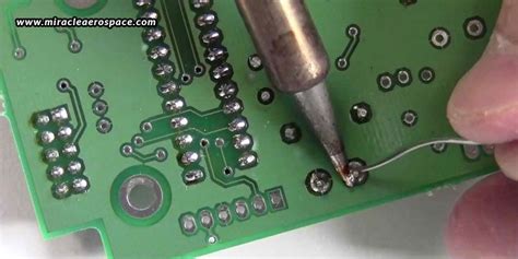
Through-hole technology, also known as thru-hole technology or leaded technology, is a method used in printed circuit board (PCB) fabrication where component leads are inserted into drilled holes and soldered to pads on the opposite side of the board. This technology has been widely used in the electronics industry for decades and continues to be a reliable method for mounting components onto PCBs.
Advantages of Through-hole Technology
- Strong mechanical bonds: Through-hole components provide a strong mechanical connection between the component and the PCB, making them more resistant to vibration and physical stress.
- Easier manual assembly: Through-hole components are easier to work with during manual assembly processes, as they can be inserted and soldered by hand.
- Better thermal management: The leads of through-hole components can dissipate heat more effectively than surface-mount components, as they have a larger surface area in contact with the PCB.
- Suitable for high-power applications: Through-hole technology is often used for high-power components, such as transformers and power transistors, due to their ability to handle higher currents and voltages.
Disadvantages of Through-hole Technology
- Larger PCB size: Through-hole components require drilling holes and take up more space on the PCB, resulting in larger board sizes compared to surface-mount technology (SMT).
- Higher production costs: The drilling process and the need for more raw materials (e.g., solder) can increase production costs compared to SMT.
- Slower assembly process: Inserting and soldering through-hole components is generally slower than placing and soldering surface-mount components, especially in automated assembly lines.
- Limited component density: Due to the larger size of through-hole components and the need for drilled holes, the component density on a PCB is lower compared to SMT.
Through-hole PCB Fabrication Process
The through-hole PCB fabrication process involves several steps, which are outlined below:
-
PCB Design: The PCB design is created using electronic design automation (EDA) software, which includes the placement of through-hole components and the routing of traces.
-
Drilling: Holes are drilled into the PCB substrate at the locations specified in the PCB design. The drilling process can be done using automated CNC machines or manual drilling equipment.
-
Plating: After drilling, the holes are plated with a conductive material, typically copper, to create an electrical connection between the layers of the PCB. This process is known as electroplating.
-
Solder Mask Application: A solder mask is applied to the PCB to protect the copper traces from oxidation and to prevent solder bridges from forming during the soldering process. The solder mask also helps to identify the component placement locations.
-
Silkscreen Printing: A silkscreen layer is printed onto the PCB to add labels, logos, and other identifiers. This layer helps with the assembly process and provides a professional appearance to the finished product.
-
Component Placement: Through-hole components are inserted into the drilled holes on the PCB. This process can be done manually or using automated insertion machines.
-
Soldering: The PCB is then sent through a wave soldering machine, which applies molten solder to the bottom of the board, creating a secure electrical and mechanical connection between the component leads and the PCB pads.
-
Inspection and Testing: After soldering, the PCB undergoes a visual inspection and electrical testing to ensure that all connections are properly made and that the board functions as intended.
Comparison of Through-hole and Surface-mount Technology
| Characteristic | Through-hole Technology | Surface-mount Technology |
|---|---|---|
| Component size | Larger | Smaller |
| PCB size | Larger | Smaller |
| Component density | Lower | Higher |
| Assembly process | Slower, manual or automated | Faster, mostly automated |
| Mechanical strength | Stronger | Weaker |
| Thermal management | Better | Worse |
| Suitable applications | High-power, high-reliability | High-density, portable devices |
| Production costs | Higher | Lower |

Applications of Through-hole Technology
Despite the growing popularity of surface-mount technology, through-hole technology remains essential in various applications, such as:
-
High-power electronics: Power supplies, inverters, and motor controllers often use through-hole components due to their ability to handle high currents and voltages.
-
Aerospace and military: These industries require high-reliability electronics that can withstand harsh environments, making through-hole technology a preferred choice.
-
Prototype and low-volume production: Through-hole components are easier to work with during manual assembly, making them suitable for prototyping and low-volume production runs.
-
Hobbyist and educational projects: DIY enthusiasts and students often use through-hole components in their projects due to their ease of use and the availability of through-hole component kits.
Future of Through-hole Technology
While surface-mount technology has become increasingly popular in recent years, through-hole technology is likely to remain relevant in specific applications. Some factors that contribute to the continued use of through-hole technology include:
-
Technological advancements: Improvements in through-hole component design and PCB fabrication processes can help to minimize some of the disadvantages associated with this technology, such as larger PCB sizes and higher production costs.
-
Industry-specific requirements: Certain industries, such as aerospace and military, may continue to rely on through-hole technology due to its proven reliability and ability to withstand harsh environments.
-
Hybrid PCBs: Many modern PCB designs incorporate both through-hole and surface-mount components, leveraging the advantages of each technology. This trend is likely to continue as designers seek to optimize PCB performance, reliability, and cost-effectiveness.
Frequently Asked Questions (FAQ)
-
Q: Can through-hole and surface-mount components be used on the same PCB?
A: Yes, it is possible to design a PCB that incorporates both through-hole and surface-mount components. This is known as a hybrid PCB design and can offer the benefits of both technologies. -
Q: Are through-hole components more expensive than surface-mount components?
A: In general, through-hole components are less expensive than their surface-mount counterparts. However, the overall cost of a PCB depends on various factors, such as the number of components, PCB size, and production volume. -
Q: Can through-hole PCBs be assembled using automated processes?
A: Yes, through-hole PCBs can be assembled using automated insertion machines and wave soldering equipment. However, the assembly process is generally slower compared to surface-mount technology. -
Q: Are through-hole components becoming obsolete?
A: While surface-mount technology has gained popularity, through-hole components are still widely used in various applications, particularly in high-power electronics, aerospace, and military industries. Through-hole technology is likely to remain relevant in the foreseeable future. -
Q: What are the main advantages of using through-hole technology in PCB fabrication?
A: The main advantages of using through-hole technology include stronger mechanical bonds, easier manual assembly, better thermal management, and suitability for high-power applications.
In conclusion, through-hole technology remains an essential aspect of PCB fabrication, offering unique advantages in terms of mechanical strength, thermal management, and suitability for high-power applications. While surface-mount technology has become increasingly popular, through-hole components are likely to remain relevant in specific industries and applications. As PCB designers continue to innovate and develop new techniques, it is expected that through-hole technology will evolve to meet the changing needs of the electronics industry.
Leave a Reply