Introduction to PCB-OSP
Printed Circuit Boards (PCBs) are essential components in modern electronics, providing a platform for electrical components to be mounted and interconnected. With the increasing demand for environmentally friendly manufacturing processes, the use of Organic Solderability Preservatives (OSP) has gained popularity in the PCB industry. OSP is a surface finish that protects the copper pads on PCBs from oxidation and ensures good solderability during the assembly process.
What is OSP?
OSP is a chemical coating applied to the exposed copper surfaces of a PCB to prevent oxidation and maintain solderability. It is an alternative to other surface finishes such as Hot Air Solder Leveling (HASL), Electroless Nickel Immersion Gold (ENIG), and Immersion Silver. OSP is a cost-effective and environmentally friendly option that provides excellent solderability and shelf life for PCBs.
Advantages of using OSP in PCB manufacturing
-
Environment-friendly: OSP is a non-toxic and biodegradable surface finish that does not contain heavy metals or hazardous chemicals. It is RoHS (Restriction of Hazardous Substances) compliant and meets environmental regulations.
-
Cost-effective: Compared to other surface finishes, OSP is a cost-effective solution for PCB manufacturing. It requires fewer processing steps and materials, resulting in lower production costs.
-
Excellent solderability: OSP provides excellent solderability by protecting the copper pads from oxidation. It ensures good wetting and spreading of solder during the assembly process, resulting in reliable solder joints.
-
Good shelf life: PCBs with OSP surface finish have a good shelf life, typically up to 12 months when stored properly. This allows for flexibility in production planning and inventory management.
-
Compatibility with different soldering methods: OSP is compatible with various soldering methods, including wave soldering, reflow soldering, and hand soldering. It can be used with both lead-based and lead-free solder alloys.
Types of OSP
There are two main types of OSP used in PCB manufacturing: Imidazole-based OSP and Benzimidazole-based OSP.
Imidazole-based OSP
Imidazole-based OSP is the most common type of OSP used in the PCB industry. It is a water-based solution that contains imidazole compounds as the main active ingredients. Imidazole-based OSP forms a thin, uniform coating on the copper surface, providing excellent protection against oxidation and ensuring good solderability.
Advantages of Imidazole-based OSP
-
Fast curing time: Imidazole-based OSP has a fast curing time, typically around 10-15 minutes at a temperature of 150-180°C. This allows for faster production throughput and reduced energy consumption.
-
Good thermal stability: Imidazole-based OSP has good thermal stability and can withstand multiple reflow cycles without significant degradation of the coating.
-
Excellent wetting properties: Imidazole-based OSP provides excellent wetting properties, ensuring good solder joint formation during the assembly process.
Benzimidazole-based OSP
Benzimidazole-based OSP is another type of OSP that uses benzimidazole compounds as the main active ingredients. It is a newer development in OSP technology and offers some advantages over imidazole-based OSP.
Advantages of Benzimidazole-based OSP
-
Improved thermal stability: Benzimidazole-based OSP has better thermal stability compared to imidazole-based OSP. It can withstand higher temperatures and multiple reflow cycles without significant degradation of the coating.
-
Enhanced corrosion resistance: Benzimidazole-based OSP provides better corrosion resistance, especially against acidic environments. This makes it suitable for applications in harsh environmental conditions.
-
Longer shelf life: PCBs with benzimidazole-based OSP have a longer shelf life, typically up to 18 months when stored properly. This allows for greater flexibility in production planning and inventory management.

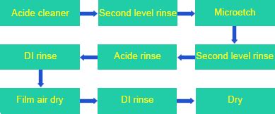
OSP Application Process
The OSP application process involves several steps to ensure a uniform and reliable coating on the PCB surface.
Pre-treatment
Before applying OSP, the PCB surface must be thoroughly cleaned and activated to ensure good adhesion of the coating. The pre-treatment process typically involves the following steps:
-
Cleaning: The PCB surface is cleaned using a mild alkaline solution to remove any contaminants, such as dirt, grease, and oxidation.
-
Microetching: A microetching solution is used to remove a thin layer of copper from the surface, creating a uniform and active surface for OSP adhesion.
-
Rinsing: The PCB is rinsed with deionized water to remove any residual chemicals from the cleaning and microetching steps.
OSP Application
After pre-treatment, the OSP solution is applied to the PCB surface using one of the following methods:
-
Dip coating: The PCB is dipped into a tank containing the OSP solution for a specified time, typically 30-60 seconds. This method ensures uniform coverage of the OSP on the PCB surface.
-
Spray coating: The OSP solution is sprayed onto the PCB surface using a spray nozzle. This method is suitable for selective application of OSP on specific areas of the PCB.
Curing
After the OSP application, the PCB is subjected to a curing process to remove any excess moisture and to crosslink the OSP coating. The curing process typically involves the following steps:
-
Pre-drying: The PCB is pre-dried using hot air or infrared radiation to remove excess moisture from the OSP coating.
-
Curing: The PCB is heated to a temperature of 150-180°C for a specified time, typically 10-15 minutes. This step crosslinks the OSP coating and improves its adhesion to the copper surface.
-
Cooling: The PCB is allowed to cool down to room temperature before further processing or packaging.

Quality Control and Testing
To ensure the reliability and performance of PCBs with OSP surface finish, various quality control and testing methods are employed.
Visual Inspection
Visual inspection is the first step in quality control, where the PCB surface is examined for any defects or irregularities in the OSP coating. Common defects include:
- Uneven coating thickness
- Pinholes or voids in the coating
- Contamination or debris on the surface
- Discoloration or staining of the coating
Thickness Measurement
The thickness of the OSP coating is a critical parameter that affects its performance and reliability. The typical thickness range for OSP coatings is 0.2-0.5 µm. Thickness measurement can be done using various methods, such as:
- X-ray fluorescence (XRF) spectroscopy
- Scanning electron microscopy (SEM) with energy-dispersive X-ray spectroscopy (EDS)
- Coulometric thickness measurement
| Method | Advantages | Disadvantages |
|---|---|---|
| XRF | Non-destructive, fast, accurate | Requires calibration, limited to flat surfaces |
| SEM/EDS | High resolution, elemental analysis | Destructive, time-consuming, expensive |
| Coulometric | Accurate, suitable for small areas | Destructive, slow, requires skilled operators |
Solderability Testing
Solderability testing is performed to evaluate the wetting and spreading properties of solder on the OSP-coated surface. Common solderability tests include:
- Wetting balance test: Measures the wetting force and time of a solder meniscus on the PCB surface.
- Dip and look test: Involves dipping the PCB in a solder bath and visually inspecting the solder coverage and wetting properties.
- Spread test: Measures the spread area of a solder paste deposit on the PCB surface after reflow.
| Test | Parameter | Typical Value |
|---|---|---|
| Wetting balance | Wetting force | > 2 mN/mm |
| Wetting time | < 2 seconds | |
| Dip and look | Solder coverage | > 95% |
| Spread | Spread area | > 80% |
Ionic Contamination Testing
Ionic contamination testing is performed to detect any ionic impurities on the PCB surface that can lead to corrosion and reliability issues. The most common method for ionic contamination testing is the resistivity of solvent extract (ROSE) test, where the PCB is immersed in a solvent, and the resistivity of the extract is measured. The acceptable limit for ionic contamination is typically less than 1.56 µg/cm².

Environmental Impact and Sustainability
One of the main advantages of OSP is its environmental friendliness compared to other surface finishes. OSP is RoHS compliant and does not contain any hazardous substances, such as lead, cadmium, or hexavalent chromium. This makes it a sustainable choice for PCB manufacturing, reducing the environmental impact of electronic products.
Comparison with other surface finishes
| Surface Finish | Environmental Impact | RoHS Compliance |
|---|---|---|
| OSP | Low | Yes |
| HASL | High (lead content) | No |
| ENIG | Moderate (nickel and gold) | Yes |
| Immersion Silver | Low | Yes |
Waste Management and Recycling
Proper waste management and recycling practices are essential to minimize the environmental impact of PCB manufacturing. OSP-coated PCBs can be recycled using various methods, such as:
- Mechanical recycling: PCBs are shredded, and the metal content is separated using magnetic and density separation techniques.
- Chemical recycling: PCBs are chemically treated to dissolve the metals, which are then recovered using electrowinning or precipitation methods.
- Thermal recycling: PCBs are incinerated, and the metals are recovered from the ash using pyrometallurgical processes.
Future Trends and Developments
As the demand for environmentally friendly and sustainable electronics continues to grow, the use of OSP in PCB manufacturing is expected to increase. Some of the future trends and developments in OSP technology include:
-
Improved formulations: Researchers are developing new OSP formulations with enhanced properties, such as better thermal stability, longer shelf life, and improved corrosion resistance.
-
Selective OSP application: Advances in OSP application methods, such as inkjet printing and laser-assisted deposition, are enabling selective application of OSP on specific areas of the PCB, reducing material consumption and cost.
-
Integration with other surface finishes: OSP can be used in combination with other surface finishes, such as ENIG or immersion silver, to provide additional benefits, such as improved wire bonding or high-frequency performance.
-
Eco-friendly packaging: The development of biodegradable and compostable packaging materials for OSP-coated PCBs can further reduce the environmental impact of electronic products.
Frequently Asked Questions (FAQ)
-
Q: What is the shelf life of OSP-coated PCBs?
A: The shelf life of OSP-coated PCBs is typically 12 months for imidazole-based OSP and up to 18 months for benzimidazole-based OSP when stored properly in a cool, dry environment. -
Q: Can OSP be used for high-frequency applications?
A: Yes, OSP can be used for high-frequency applications, as it provides a smooth and uniform surface that minimizes signal loss and distortion. However, for critical high-frequency applications, other surface finishes like ENIG or immersion silver may be preferred. -
Q: Is OSP suitable for wire bonding?
A: OSP is not recommended for wire bonding, as the thin organic layer may not provide sufficient bonding strength and reliability. For applications requiring wire bonding, surface finishes like ENIG or electroless nickel electroless palladium immersion gold (ENEPIG) are preferred. -
Q: How does OSP compare to HASL in terms of cost?
A: OSP is generally more cost-effective than HASL, as it requires fewer processing steps and materials. Additionally, the environmental and health hazards associated with lead-based HASL make OSP a more attractive option for PCB manufacturers. -
Q: Can OSP be reworked or repaired?
A: Yes, OSP-coated PCBs can be reworked or repaired using standard soldering techniques. However, care must be taken to ensure that the rework process does not damage the OSP coating or the underlying copper surface. After rework, the repaired area may need to be recoated with OSP to maintain solderability and protection.
Conclusion
OSP is an environmentally friendly and cost-effective surface finish for PCBs that provides excellent solderability and protection against oxidation. With the increasing focus on sustainability and RoHS compliance in the electronics industry, the use of OSP in PCB manufacturing is expected to grow. By understanding the advantages, application process, quality control methods, and environmental impact of OSP, PCB manufacturers can make informed decisions and contribute to a greener future for the electronics industry.
As new formulations and application methods are developed, OSP will continue to evolve and meet the ever-changing needs of the PCB industry. By adopting OSP and other eco-friendly manufacturing practices, PCB manufacturers can not only reduce their environmental footprint but also stay competitive in a market that increasingly values sustainability and social responsibility.


Leave a Reply