Introduction to PCB Solder Mask
Printed Circuit Boards (PCBs) are essential components in modern electronic devices. They provide a platform for mounting and interconnecting electronic components, ensuring proper functionality and reliability. One crucial aspect of PCB manufacturing is the application of solder mask, also known as solder resist or solder stop mask. In this article, we will explore the various functions of solder mask in PCBs and how it contributes to the overall performance and longevity of electronic devices.
What is Solder Mask?
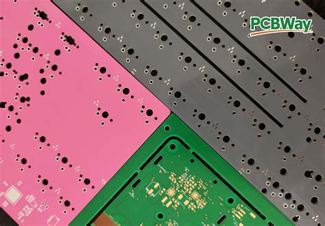
Solder mask is a thin layer of polymer coating applied to the copper traces and pads on a PCB, leaving only the areas that need to be soldered exposed. It is typically green in color but can also be found in other colors such as red, blue, black, or white. The primary purpose of solder mask is to protect the copper traces from oxidation, prevent solder bridges, and provide electrical insulation between adjacent traces and components.
Functions of Solder Mask in PCB
1. Protection against Oxidation
One of the primary functions of solder mask is to protect the copper traces on a PCB from oxidation. Copper is prone to oxidation when exposed to air, which can lead to the formation of copper oxide on the surface. This oxidation can cause issues with solderability and electrical conductivity, ultimately affecting the performance and reliability of the PCB. By covering the copper traces with solder mask, the exposure to air is minimized, preventing oxidation and ensuring proper functionality of the circuit board.
2. Prevention of Solder Bridges
Solder bridges are unintended connections between two or more solder joints, which can occur during the soldering process. These bridges can cause short circuits and lead to malfunction or failure of the electronic device. Solder mask helps prevent solder bridges by covering the areas between adjacent pads and traces, leaving only the intended solder points exposed. This selective exposure ensures that solder only adheres to the desired locations, minimizing the risk of unwanted connections.
3. Electrical Insulation
Solder mask provides electrical insulation between adjacent traces and components on a PCB. By covering the copper traces, solder mask acts as a dielectric layer, preventing current from flowing between adjacent traces and reducing the risk of short circuits. This insulation is particularly important in high-density PCBs where the spacing between traces is minimal. Solder mask helps maintain the integrity of the electrical signals and prevents interference or crosstalk between different parts of the circuit.
4. Improved Solderability
Solder mask plays a crucial role in improving the solderability of a PCB. By selectively exposing only the areas that need to be soldered, solder mask ensures that solder flows smoothly and adheres properly to the exposed pads and traces. The solder mask creates a dam-like structure around the exposed areas, preventing the solder from spreading beyond the intended location. This controlled flow of solder results in cleaner and more reliable solder joints, enhancing the overall quality of the soldering process.
5. Enhanced Durability and Protection
Solder mask provides an additional layer of protection to the PCB, enhancing its durability and longevity. The polymer coating acts as a barrier against physical damage, scratches, and abrasions that can occur during handling, assembly, or use of the electronic device. Solder mask also offers protection against environmental factors such as moisture, dust, and chemicals, which can potentially damage the PCB or cause corrosion of the copper traces. By shielding the PCB from these external factors, solder mask helps extend the lifespan of the electronic device.
6. Improved Aesthetics
In addition to its functional benefits, solder mask also contributes to the aesthetic appeal of a PCB. The uniform coating of solder mask gives the PCB a professional and polished look, enhancing its visual appearance. Solder mask can be applied in various colors, allowing for customization and branding of the PCB. The color of the solder mask can also serve as a visual aid for identifying different components or sections of the circuit board, making it easier for technicians to navigate and troubleshoot the device.
7. Facilitates Automated Assembly
Solder mask plays a significant role in facilitating automated assembly processes for PCBs. The selective exposure of solder pads and traces enables the use of automated soldering techniques such as wave soldering or reflow soldering. The solder mask acts as a guide for the automated equipment, ensuring precise and accurate placement of solder on the exposed areas. This automation reduces human error, increases production efficiency, and enables the manufacturing of large quantities of PCBs with consistent quality.

Types of Solder Mask
There are two main types of solder mask used in PCB manufacturing: liquid photoimageable solder mask (LPISM) and dry film solder mask (DFSM).
Liquid Photoimageable Solder Mask (LPISM)
LPISM is the most commonly used type of solder mask in PCB manufacturing. It is applied as a liquid coating onto the PCB and then exposed to UV light through a photomask. The areas exposed to UV light cure and harden, while the unexposed areas remain soluble and can be washed away, leaving the desired solder mask pattern. LPISM offers high resolution, excellent adhesion, and good thermal and chemical resistance.
Dry Film Solder Mask (DFSM)
DFSM is an alternative to LPISM and is applied as a thin, dry film onto the PCB. The film is then exposed to UV light through a photomask, and the unexposed areas are removed using a chemical developer. DFSM provides a uniform thickness and is suitable for high-volume production. However, it may not offer the same level of resolution and adhesion as LPISM.
| Type of Solder Mask | Application Method | Advantages | Disadvantages |
|---|---|---|---|
| LPISM | Liquid coating | High resolution, excellent adhesion, good thermal and chemical resistance | Requires precise control of coating thickness |
| DFSM | Dry film | Uniform thickness, suitable for high-volume production | Lower resolution and adhesion compared to LPISM |

Solder Mask Application Process
The application of solder mask involves several steps to ensure a high-quality and reliable coating on the PCB. The general process for applying solder mask is as follows:
-
PCB Cleaning: The PCB is thoroughly cleaned to remove any contaminants, dirt, or residues that may affect the adhesion of the solder mask.
-
Solder Mask Application: The solder mask is applied to the PCB either as a liquid coating (LPISM) or a dry film (DFSM). The coating is evenly distributed across the surface of the PCB.
-
UV Exposure: The PCB with the applied solder mask is exposed to UV light through a photomask. The photomask contains the desired pattern for the solder mask, and the UV light cures and hardens the exposed areas.
-
Developing: After UV exposure, the unexposed areas of the solder mask are removed using a chemical developer. This step reveals the copper pads and traces that need to be exposed for soldering.
-
Curing: The PCB undergoes a final curing process to fully harden the solder mask and improve its adhesion to the copper surface. This is typically done using heat or UV light.
-
Inspection: The PCB is inspected for any defects or imperfections in the solder mask coating. Any issues are addressed before proceeding to the next stage of PCB assembly.

Frequently Asked Questions (FAQ)
-
What is the purpose of solder mask on a PCB?
The purpose of solder mask on a PCB is to protect the copper traces from oxidation, prevent solder bridges, provide electrical insulation, improve solderability, enhance durability, and facilitate automated assembly processes. -
Can solder mask be applied in different colors?
Yes, solder mask can be applied in various colors such as green, red, blue, black, or white. The choice of color depends on the specific requirements of the PCB and the preferences of the manufacturer or customer. -
What is the difference between LPISM and DFSM?
LPISM (Liquid Photoimageable Solder Mask) is applied as a liquid coating and offers high resolution, excellent adhesion, and good thermal and chemical resistance. DFSM (Dry Film Solder Mask) is applied as a thin, dry film and provides uniform thickness, making it suitable for high-volume production. However, DFSM may have lower resolution and adhesion compared to LPISM. -
Is solder mask necessary for all PCBs?
While solder mask is highly recommended for most PCBs, there may be some specific applications where it is not necessary. For example, in very low-cost or disposable PCBs where the risk of oxidation or solder bridges is minimal, solder mask may be omitted to reduce manufacturing costs. -
Can solder mask be removed or reworked if needed?
Yes, solder mask can be removed or reworked if necessary. However, it is a delicate process that requires special tools and techniques to avoid damaging the underlying copper traces. Rework should only be performed by experienced technicians to ensure the integrity of the PCB is maintained.
Conclusion
Solder mask is a vital component in the manufacturing of printed circuit boards (PCBs). Its primary functions include protecting copper traces from oxidation, preventing solder bridges, providing electrical insulation, improving solderability, enhancing durability, and facilitating automated assembly processes. The two main types of solder mask, LPISM and DFSM, offer different advantages and are selected based on specific PCB requirements.
The application of solder mask involves a multi-step process that ensures a high-quality and reliable coating on the PCB. From cleaning and applying the solder mask to UV exposure, developing, curing, and inspection, each step plays a crucial role in achieving the desired results.
Understanding the functions and importance of solder mask is essential for anyone involved in PCB design, manufacturing, or assembly. By leveraging the benefits of solder mask, manufacturers can produce PCBs that are more reliable, durable, and visually appealing, ultimately contributing to the overall quality and performance of electronic devices.
As technology continues to advance and the demand for high-density, high-performance PCBs grows, the role of solder mask will remain critical. Ongoing research and development in solder mask materials and application techniques will further enhance its capabilities and ensure that PCBs can meet the evolving needs of the electronics industry.


Leave a Reply