Introduction to PCB Solder Mask
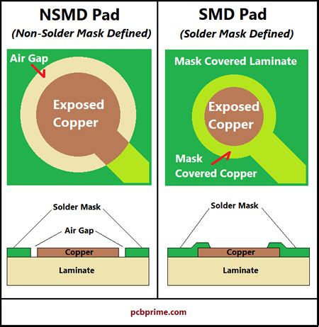
Printed Circuit Boards (PCBs) are essential components in modern electronics, providing a platform for electrical components to be mounted and connected. One crucial aspect of PCB manufacturing is the application of a solder mask, which serves several important functions. A PCB solder mask is a thin layer of polymer that is applied to the copper traces of a PCB, leaving only the areas that need to be soldered exposed.
The primary purpose of a solder mask is to protect the copper traces from oxidation and prevent solder bridges from forming between adjacent traces during the soldering process. Additionally, solder masks provide electrical insulation, improve the PCB’s appearance, and help users identify different components and features on the board.
Importance of Solder Mask in PCB Manufacturing
Solder masks play a vital role in PCB manufacturing, offering numerous benefits that contribute to the overall quality, reliability, and functionality of the final product. Some of the key advantages of using a solder mask include:
-
Protection against oxidation: Copper traces on a PCB can easily oxidize when exposed to air, leading to reduced conductivity and potential signal loss. By covering the traces with a solder mask, the copper is protected from oxidation, ensuring optimal performance and longevity.
-
Prevention of solder bridges: During the soldering process, molten solder can inadvertently flow between adjacent traces, creating unintended connections known as solder bridges. These bridges can cause short circuits and other functional issues. Solder masks help prevent this by covering the areas between traces, minimizing the risk of solder bridges forming.
-
Electrical insulation: Solder masks act as electrical insulators, preventing current from flowing between traces that are not meant to be connected. This insulation is crucial for maintaining the integrity of the PCB’s electrical circuits and preventing signal interference.
-
Improved aesthetics: Solder masks are available in various colors, with green being the most common. The uniform color of the solder mask enhances the visual appeal of the PCB and makes it easier for users to identify different components and features on the board.
-
Increased durability: Solder masks provide an additional layer of protection for the PCB, shielding it from physical damage, dust, and debris. This added durability helps extend the lifespan of the PCB and reduces the risk of failures caused by environmental factors.
Types of PCB Solder Mask
There are several types of solder masks used in PCB manufacturing, each with its own unique properties and advantages. The four main types of PCB solder mask are:
- Liquid Photo-Imageable (LPI) Solder Mask
- Dry Film Solder Mask
- Peelable Solder Mask
- Thermal Cure Solder Mask
1. Liquid Photo-Imageable (LPI) Solder Mask
Liquid Photo-Imageable (LPI) solder mask is the most widely used type of solder mask in PCB manufacturing. LPI solder mask is a photosensitive polymer that is applied to the PCB surface in liquid form, typically through screen printing or spraying. Once applied, the LPI solder mask is exposed to UV light through a photomask, which hardens the exposed areas while leaving the unexposed areas soluble.
After exposure, the PCB is developed in a chemical solution, removing the unexposed portions of the solder mask and revealing the copper traces that need to be soldered. LPI solder mask offers several advantages, including:
- High resolution and precision
- Excellent adhesion to the PCB surface
- Durability and resistance to chemicals and abrasion
- Wide range of available colors
- Cost-effectiveness for high-volume production
However, LPI solder mask does have some limitations. The application process can be time-consuming, and the mask may not be suitable for high-temperature applications due to its lower thermal resistance compared to other types of solder masks.
Application Process for LPI Solder Mask
The application process for LPI solder mask involves several steps:
-
Cleaning: The PCB surface is thoroughly cleaned to remove any dirt, grease, or contaminants that could affect the adhesion of the solder mask.
-
Application: The liquid solder mask is applied to the PCB surface using screen printing or spraying techniques. The thickness of the applied mask is typically between 0.5 and 1.5 mils (12.7 to 38.1 microns).
-
Pre-drying: The PCB is pre-dried to remove any excess solvent from the solder mask and to improve its stability during the exposure process.
-
Exposure: The PCB is exposed to UV light through a photomask, which hardens the exposed areas of the solder mask while leaving the unexposed areas soluble.
-
Developing: The PCB is developed in a chemical solution, removing the unexposed portions of the solder mask and revealing the copper traces that need to be soldered.
-
Curing: The PCB is then cured at a high temperature (typically 150°C) to fully harden the solder mask and ensure its durability and resistance to chemicals and abrasion.
2. Dry Film Solder Mask
Dry film solder mask is a photosensitive polymer that comes in the form of a thin, solid film. The film is laminated onto the PCB surface using heat and pressure, and then exposed to UV light through a photomask. The exposed areas of the film become cross-linked and insoluble, while the unexposed areas remain soluble and can be removed during the developing process.
Dry film solder mask offers several advantages over LPI solder mask:
- Faster application process
- Higher thermal resistance
- Better conformity to surface irregularities
- Improved adhesion to the PCB surface
However, dry film solder mask has some limitations, including:
- Higher cost compared to LPI solder mask
- Limited color options
- Potential for air entrapment during lamination
- Difficulty in achieving fine pitch features
Application Process for Dry Film Solder Mask
The application process for dry film solder mask involves several steps:
-
Cleaning: The PCB surface is thoroughly cleaned to remove any dirt, grease, or contaminants that could affect the adhesion of the solder mask.
-
Lamination: The dry film solder mask is laminated onto the PCB surface using heat and pressure. The lamination process typically occurs at temperatures between 80°C and 120°C, with pressure ranging from 2 to 5 bar.
-
Exposure: The PCB is exposed to UV light through a photomask, which cross-links and hardens the exposed areas of the film while leaving the unexposed areas soluble.
-
Developing: The PCB is developed in a chemical solution, removing the unexposed portions of the solder mask and revealing the copper traces that need to be soldered.
-
Post-curing: The PCB is then post-cured at a high temperature (typically 150°C to 160°C) to fully harden the solder mask and ensure its durability and resistance to chemicals and abrasion.
3. Peelable Solder Mask
Peelable solder mask is a temporary, removable solder mask that is used to protect specific areas of a PCB during the soldering process. This type of solder mask is typically applied manually or by using a dispensing machine. After soldering, the peelable mask can be easily removed, leaving the protected areas clean and free of solder.
Peelable solder mask is particularly useful in situations where components need to be soldered onto the PCB after the main soldering process has been completed, such as when adding test points or connectors. It is also used in prototype development and small-scale production, where the flexibility to make changes to the PCB design is essential.
Advantages of peelable solder mask include:
- Easy application and removal
- Flexibility in design changes
- Protection of specific areas during soldering
- Cost-effectiveness for small-scale production and prototyping
However, peelable solder mask has some limitations:
- Not suitable for high-volume production
- Limited durability and resistance to chemicals and abrasion
- Potential for residue left on the PCB surface after removal
Application Process for Peelable Solder Mask
The application process for peelable solder mask is relatively simple:
-
Cleaning: The PCB surface is cleaned to remove any dirt, grease, or contaminants that could affect the adhesion of the solder mask.
-
Application: The peelable solder mask is applied manually or using a dispensing machine to the specific areas of the PCB that need to be protected during soldering.
-
Drying: The PCB is allowed to dry, typically at room temperature, to ensure that the peelable mask adheres properly to the surface.
-
Soldering: The PCB undergoes the soldering process, with the peelable mask protecting the designated areas from solder.
-
Removal: After soldering, the peelable mask is carefully removed by peeling it off the PCB surface, leaving the protected areas clean and free of solder.
4. Thermal Cure Solder Mask
Thermal cure solder mask is a type of solder mask that is cured using heat instead of UV light. This solder mask is applied to the PCB surface in liquid form, typically through screen printing or spraying, and then cured at a high temperature (usually between 130°C and 150°C) to harden and cross-link the polymer.
Thermal cure solder mask offers several advantages:
- Excellent thermal resistance
- Good chemical resistance
- High durability and abrasion resistance
- Cost-effectiveness for high-volume production
However, thermal cure solder mask has some limitations:
- Longer curing time compared to UV-cured solder masks
- Potential for warping or deformation of the PCB due to high curing temperatures
- Limited color options
Application Process for Thermal Cure Solder Mask
The application process for thermal cure solder mask involves several steps:
-
Cleaning: The PCB surface is thoroughly cleaned to remove any dirt, grease, or contaminants that could affect the adhesion of the solder mask.
-
Application: The thermal cure solder mask is applied to the PCB surface using screen printing or spraying techniques. The thickness of the applied mask is typically between 0.5 and 1.5 mils (12.7 to 38.1 microns).
-
Pre-drying: The PCB is pre-dried to remove any excess solvent from the solder mask and to improve its stability during the curing process.
-
Curing: The PCB is cured at a high temperature (typically between 130°C and 150°C) for a specified duration to fully harden and cross-link the solder mask.
Comparison of Solder Mask Types
| Solder Mask Type | Advantages | Disadvantages |
|---|---|---|
| Liquid Photo-Imageable (LPI) | High resolution and precision, excellent adhesion, wide range of colors, cost-effective for high-volume production | Time-consuming application process, lower thermal resistance |
| Dry Film | Faster application process, higher thermal resistance, better conformity to surface irregularities | Higher cost, limited color options, potential for air entrapment during lamination |
| Peelable | Easy application and removal, flexibility in design changes, cost-effective for small-scale production and prototyping | Not suitable for high-volume production, limited durability and resistance to chemicals and abrasion |
| Thermal Cure | Excellent thermal resistance, good chemical resistance, high durability, cost-effective for high-volume production | Longer curing time, potential for PCB warping or deformation, limited color options |

Frequently Asked Questions (FAQ)
1. What is the most common color for PCB solder masks?
The most common color for PCB solder masks is green. However, solder masks are available in a variety of colors, including blue, red, yellow, black, and white.
2. Can solder mask be applied to both sides of a PCB?
Yes, solder mask can be applied to both sides of a PCB. This is common practice, especially for double-sided and multi-layer PCBs, to protect the copper traces on all layers and prevent solder bridging.
3. How does solder mask affect the assembly process?
Solder mask plays a crucial role in the assembly process by exposing only the areas of the PCB that need to be soldered, such as pads and vias. This helps to prevent solder bridges and ensures that components are properly connected to the correct points on the board.
4. What is the typical thickness of a solder mask?
The typical thickness of a solder mask ranges from 0.5 to 1.5 mils (12.7 to 38.1 microns). The thickness can vary depending on the type of solder mask and the specific requirements of the PCB design.
5. Are there any environmental concerns associated with solder masks?
Some solder masks may contain harmful chemicals that can have negative environmental impacts if not disposed of properly. However, many PCB manufacturers now use environmentally friendly, RoHS-compliant solder masks that minimize these concerns. It is essential to work with reputable PCB manufacturers that adhere to environmental regulations and best practices.
Conclusion
Solder masks are an essential component of PCB manufacturing, providing protection, insulation, and improved aesthetics to the finished board. The four main types of PCB solder mask – liquid photo-imageable, dry film, peelable, and thermal cure – each offer unique advantages and disadvantages, making them suitable for different applications and production scales.
When selecting a solder mask for a PCB design, it is essential to consider factors such as the required resolution and precision, thermal and chemical resistance, durability, and cost-effectiveness. By understanding the properties and application processes of each solder mask type, PCB designers and manufacturers can make informed decisions that ensure the optimal performance, reliability, and longevity of their products.
As PCB technology continues to evolve, so too will the development of new and improved solder mask materials and application techniques. By staying up-to-date with these advancements, the electronics industry can continue to push the boundaries of what is possible in PCB design and manufacturing, while also prioritizing environmental sustainability and user safety.
Leave a Reply