How Solder Mask Dam Works
The solder mask dam technique is implemented during the PCB manufacturing process. Here’s a step-by-step explanation of how it works:
-
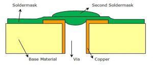
PCB Design: During the PCB design phase, the copper pads for components are defined with a specific size and shape. The solder mask layer is then designed to cover the majority of the PCB surface, leaving openings for the copper pads.
-
Solder Mask Application: The solder mask material, typically a liquid photoimageable polymer, is applied to the PCB surface. This material is usually green in color but can also be found in other colors such as blue, red, or black.
-
Solder Mask Exposure: The PCB with the applied solder mask undergoes a photolithography process. The solder mask is exposed to UV light through a photomask, which contains the desired pattern for the solder mask openings.
-
Solder Mask Development: After exposure, the PCB is subjected to a development process. The unexposed areas of the solder mask are removed, leaving openings that expose the copper pads. The exposed areas of the solder mask remain on the PCB surface.
-
Solder Mask Curing: The PCB with the developed solder mask undergoes a curing process, typically involving heat treatment. This process hardens and solidifies the solder mask material, making it durable and resistant to chemicals and environmental factors.
The resulting solder mask dam creates a raised barrier around the copper pads. This barrier is typically 0.1 to 0.15 mm high and extends beyond the edge of the copper pad by 0.05 to 0.1 mm.
Advantages of Solder Mask Dam
The use of solder mask dam offers several advantages in PCB manufacturing and assembly:
-
Improved Solder Control: The raised barrier created by the solder mask dam helps to contain the molten solder within the desired area during the soldering process. This prevents solder bridging and short circuits between adjacent pads.
-
Enhanced Solder Joint Reliability: By restricting the flow of molten solder, the solder mask dam promotes the formation of a well-defined and uniform solder joint. This improves the mechanical strength and electrical reliability of the solder connection.
-
Better Pad Definition: The solder mask dam creates a clear and precise boundary around the copper pads. This improves the visual contrast between the pads and the surrounding solder mask, making it easier for automated optical inspection (AOI) systems to detect any soldering defects.
-
Reduced Solder Defects: The controlled flow of solder within the dam minimizes the occurrence of common solder defects such as solder balls, solder splashes, and insufficient solder coverage. This leads to higher manufacturing yields and reduced rework.
-
Compatibility with Fine-Pitch Components: Solder mask dam is particularly beneficial for PCBs with fine-pitch components, such as ball grid arrays (BGAs) and chip-scale packages (CSPs). The precise control over solder flow helps to prevent short circuits and ensures reliable soldering of these small-sized components.

Design Considerations for Solder Mask Dam
When incorporating solder mask dam into PCB designs, several factors need to be considered:
-
Pad Size and Shape: The size and shape of the copper pads should be designed to accommodate the solder mask dam. The pads should be slightly larger than the component leads or contact areas to allow for proper solder mask clearance.
-
Solder Mask Clearance: The solder mask clearance, which is the distance between the edge of the copper pad and the solder mask opening, should be carefully defined. A typical solder mask clearance is 0.05 to 0.1 mm, depending on the PCB manufacturing capabilities and the component requirements.
-
Solder Mask Thickness: The thickness of the solder mask material should be considered when designing the solder mask dam. A thicker solder mask provides a higher dam and better solder containment but may impact the overall PCB thickness and component clearances.
-
Solder Paste Stencil Design: When using solder mask dam, the solder paste stencil should be designed accordingly. The stencil apertures should be aligned with the solder mask openings and sized appropriately to ensure the right amount of solder paste is deposited on the pads.
-
Assembly Process Compatibility: The solder mask dam design should be compatible with the intended assembly process, such as reflow soldering or wave soldering. The dam height and profile should allow for proper solder flow and wetting during the soldering process.

Solder Mask Dam vs. Non-Solder Mask Defined Pads
In contrast to solder mask defined pads (SMD), there is another pad design approach called non-solder mask defined pads (NSMD). In NSMD, the copper pads are not covered by solder mask material, and the solder mask opening is larger than the copper pad itself.
Here’s a comparison table highlighting the key differences between solder mask dam and non-solder mask defined pads:
| Feature | Solder Mask Dam (SMD) | Non-Solder Mask Defined (NSMD) |
|---|---|---|
| Pad Definition | Copper pad defined by solder mask opening | Copper pad not defined by solder mask |
| Solder Mask Opening | Smaller than copper pad | Larger than copper pad |
| Solder Containment | Better solder containment within the dam | Less controlled solder flow |
| Solder Joint Reliability | Higher reliability due to uniform solder joint | Potential for uneven solder joint formation |
| Pad Etching Accuracy | Less critical, as solder mask defines the pad | Requires precise etching of copper pads |
| Visual Inspection | Easier visual inspection of solder joints | More challenging to inspect solder joints |
The choice between solder mask dam and non-solder mask defined pads depends on various factors, such as the PCB design requirements, component types, manufacturing capabilities, and assembly processes.

Frequently Asked Questions (FAQ)
-
What is the purpose of solder mask dam in PCB design?
Solder mask dam is used to create a raised barrier around the copper pads on a PCB. This barrier helps to contain the molten solder within the desired area during the soldering process, preventing solder bridging and improving the reliability of solder joints. -
What materials are used for solder mask dam?
Solder mask dam is typically made from liquid photoimageable polymers, which are applied to the PCB surface and then exposed to UV light through a photomask. The most common color for solder mask is green, but other colors such as blue, red, or black are also available. -
How does solder mask dam differ from non-solder mask defined pads?
In solder mask dam (SMD), the copper pads are defined by the solder mask opening, which is smaller than the copper pad itself. In non-solder mask defined (NSMD) pads, the copper pads are not covered by solder mask, and the solder mask opening is larger than the copper pad. -
What are the advantages of using solder mask dam in PCB manufacturing?
Solder mask dam offers several advantages, including improved solder control, enhanced solder joint reliability, better pad definition, reduced solder defects, and compatibility with fine-pitch components. It helps to achieve higher manufacturing yields and reduces the need for rework. -
What design considerations should be taken into account when using solder mask dam?
When incorporating solder mask dam into PCB designs, factors such as pad size and shape, solder mask clearance, solder mask thickness, solder paste stencil design, and assembly process compatibility should be considered. Proper design ensures optimal performance and reliability of the solder mask dam technique.
In conclusion, solder mask dam is a valuable technique in PCB manufacturing that offers numerous benefits in terms of solder control, reliability, and manufacturing efficiency. By creating a raised barrier around the copper pads, solder mask dam helps to contain the molten solder, prevent defects, and enhance the overall quality of solder joints. When designing PCBs with solder mask dam, careful consideration should be given to factors such as pad size, solder mask clearance, and compatibility with the assembly process. Understanding the differences between solder mask dam and non-solder mask defined pads is also important in making informed design decisions. With the increasing demand for miniaturization and high-density PCB assemblies, solder mask dam continues to be a crucial technique in ensuring the reliability and performance of electronic devices.


Leave a Reply