Understanding Solder Mask Breakoff and Its Implications
Solder mask, also known as solder resist or solder stop, is a thin layer of polymer applied to the copper traces of a printed circuit board (PCB). Its primary function is to protect the copper traces from oxidation, prevent solder bridges from forming between closely spaced pads, and provide electrical insulation. However, solder mask bridge breakoff is a common issue faced by PCB manufacturers and assemblers, which can lead to various problems, including short circuits, poor electrical connections, and reduced reliability of the final product.
In this article, we will delve into the reasons behind solder mask bridge breaking off, its implications, and potential solutions to mitigate this issue.
What is Solder Mask Bridge Breakoff?
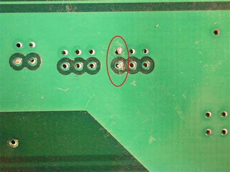
Solder mask bridge breakoff refers to the phenomenon where the solder mask material separates or breaks away from the copper traces or pads on a PCB. This can occur during the manufacturing process or during the assembly of components onto the board. When the solder mask bridge breaks off, it exposes the underlying copper, which can lead to several problems:
- Short circuits: Exposed copper traces can come into contact with each other, causing unintended electrical connections and short circuits.
- Poor solderability: Without the protection of the solder mask, the exposed copper can oxidize, making it difficult for solder to adhere properly during the assembly process.
- Reduced insulation: The absence of solder mask between closely spaced pads reduces the electrical insulation, potentially leading to signal interference or leakage.
Causes of Solder Mask Bridge Breakoff
Several factors can contribute to the occurrence of solder mask bridge breakoff. Understanding these causes is crucial for implementing preventive measures and improving the overall quality of PCBs.
1. Improper Solder Mask Application
One of the primary reasons for solder mask bridge breakoff is improper application of the solder mask material. This can happen due to various factors, such as:
- Incorrect solder mask thickness: If the solder mask is applied too thinly, it may not provide sufficient coverage and protection, making it more susceptible to breaking off. On the other hand, if the solder mask is too thick, it can cause issues with component placement and solderability.
- Uneven solder mask distribution: Inconsistent or uneven application of the solder mask can result in weak points where the material is more likely to break off.
- Contamination during application: Any contaminants present on the PCB surface or in the solder mask material itself can interfere with proper adhesion, leading to breakoff.
To address these issues, it is essential to ensure that the solder mask application process is well-controlled and optimized. This includes using the appropriate solder mask material, maintaining the correct thickness, and ensuring a clean and contaminant-free environment during application.
2. PCB Design and Layout
The design and layout of the PCB can also play a role in the occurrence of solder mask bridge breakoff. Some design-related factors to consider include:
- Pad size and spacing: If the pads on the PCB are too small or too closely spaced, it can make it challenging to achieve proper solder mask coverage. This increases the risk of solder mask bridge breakoff, especially during the assembly process when the board undergoes thermal and mechanical stresses.
- Copper trace width: Narrow copper traces can be more susceptible to solder mask bridge breakoff due to the reduced surface area for the solder mask to adhere to. Ensuring appropriate trace widths can help mitigate this issue.
- Solder mask expansion and contraction: During the manufacturing process, the PCB and solder mask undergo temperature changes, which can cause the materials to expand and contract at different rates. If the design does not account for this differential expansion, it can lead to stresses that cause the solder mask to break off.
To minimize the risk of solder mask bridge breakoff, it is crucial to follow best practices in PCB design and layout. This includes adhering to recommended pad sizes and spacing, using appropriate trace widths, and considering the thermal properties of the materials used.
3. Manufacturing Process Control
The manufacturing process itself can introduce variables that contribute to solder mask bridge breakoff. Some key process control factors include:
- Temperature and humidity: Maintaining the appropriate temperature and humidity levels during the manufacturing process is essential for proper solder mask adhesion. Excessive heat or moisture can weaken the bond between the solder mask and the copper, leading to breakoff.
- Curing and drying: Proper curing and drying of the solder mask material are critical for achieving optimal mechanical and chemical properties. Insufficient curing or drying can result in a weak solder mask layer that is more prone to breaking off.
- Handling and storage: Improper handling or storage of the PCBs during and after the manufacturing process can introduce stresses that cause the solder mask to break off. It is important to follow recommended handling and storage procedures to minimize the risk of damage.
Implementing strict process control measures and monitoring key parameters throughout the manufacturing process can help ensure the consistent quality of the solder mask and reduce the occurrence of bridge breakoff.
Implications of Solder Mask Bridge Breakoff
Solder mask bridge breakoff can have significant implications for the functionality, reliability, and longevity of PCBs. Some of the key consequences include:
1. Short Circuits and Electrical Failures
When the solder mask bridge breaks off, it exposes the underlying copper traces. If these exposed traces come into contact with each other or with other conductive materials, it can result in short circuits. Short circuits can cause a range of problems, from minor glitches to complete electrical failures, depending on the location and severity of the short.
2. Poor Solderability and Component Attachment
The solder mask not only protects the copper traces but also helps to define the areas where solder should be applied during the assembly process. When the solder mask bridge breaks off, it can lead to poor solderability, as the exposed copper may oxidize or become contaminated. This can result in weak or unreliable solder joints, which can cause components to detach or malfunction over time.
3. Reduced Insulation and Signal Integrity
The solder mask provides electrical insulation between closely spaced pads and traces. If the solder mask bridge breaks off, it reduces the insulation properties, which can lead to signal leakage, crosstalk, and electromagnetic interference (EMI). These issues can compromise the signal integrity of the PCB and affect the overall performance of the electronic device.
4. Decreased Reliability and Product Lifespan
Solder mask bridge breakoff can have a significant impact on the reliability and lifespan of the final product. Short circuits, poor solder joints, and reduced insulation can all contribute to premature failures and decreased product longevity. This can result in increased warranty claims, customer dissatisfaction, and damage to the manufacturer’s reputation.
Solutions and Prevention Strategies
To address the issue of solder mask bridge breakoff, PCB manufacturers and assemblers can implement various solutions and prevention strategies:
1. Material Selection and Qualification
Selecting the appropriate solder mask material is crucial for minimizing the risk of bridge breakoff. Some key considerations include:
- Adhesion properties: Choose a solder mask material with excellent adhesion properties to ensure a strong bond between the mask and the copper traces.
- Flexibility and durability: Opt for a solder mask material that can withstand the thermal and mechanical stresses encountered during the manufacturing and assembly processes.
- Compatibility with other materials: Ensure that the solder mask material is compatible with the other materials used in the PCB, such as the substrate, copper, and surface finishes.
Conducting thorough material qualification and testing can help identify the best solder mask material for a given application and manufacturing process.
2. Design for Manufacturability (DFM)
Incorporating DFM principles into the PCB design process can help reduce the occurrence of solder mask bridge breakoff. Some key DFM considerations include:
- Pad size and spacing: Follow recommended guidelines for pad sizes and spacing to ensure adequate solder mask coverage and minimize the risk of breakoff.
- Copper trace width: Use appropriate trace widths to provide sufficient surface area for solder mask adhesion and to reduce the likelihood of breakoff.
- Solder mask expansion and contraction: Consider the thermal properties of the solder mask material and design the PCB to accommodate differential expansion and contraction.
Collaborating closely with the PCB manufacturer and assembly team during the design phase can help identify and address potential DFM issues early in the process.
3. Process Optimization and Control
Optimizing and controlling the manufacturing process is essential for minimizing the occurrence of solder mask bridge breakoff. Some key process optimization strategies include:
- Temperature and humidity control: Implement strict control measures to maintain the appropriate temperature and humidity levels throughout the manufacturing process.
- Curing and drying: Ensure that the solder mask material is properly cured and dried according to the manufacturer’s recommendations to achieve optimal mechanical and chemical properties.
- Handling and storage: Follow best practices for handling and storing PCBs to minimize the risk of damage and solder mask breakoff.
Regular process monitoring, data collection, and analysis can help identify areas for improvement and ensure consistent quality control.
4. Inspection and Testing
Implementing robust inspection and testing procedures can help detect solder mask bridge breakoff issues early in the manufacturing process. Some common inspection and testing methods include:
- Visual inspection: Conduct thorough visual inspections of the PCBs at various stages of the manufacturing process to identify any visible solder mask defects or breakoff.
- Automated optical inspection (AOI): Use AOI systems to detect solder mask bridge breakoff and other defects accurately and efficiently.
- Electrical testing: Perform electrical tests to identify short circuits, open circuits, and other issues that may be caused by solder mask bridge breakoff.
By detecting solder mask bridge breakoff issues early, manufacturers can take corrective actions and prevent defective PCBs from reaching the assembly stage or the end customer.
Frequently Asked Questions (FAQ)
-
What is solder mask, and why is it important in PCB manufacturing?
A: Solder mask is a thin layer of polymer applied to the copper traces of a PCB. It serves several important functions, including protecting the copper from oxidation, preventing solder bridges from forming between closely spaced pads, and providing electrical insulation. Solder mask plays a crucial role in ensuring the reliability, functionality, and longevity of PCBs. -
What causes solder mask bridge breakoff, and how can it be prevented?
A: Solder mask bridge breakoff can be caused by various factors, such as improper solder mask application, PCB design and layout issues, and manufacturing process control problems. To prevent solder mask bridge breakoff, manufacturers can implement strategies such as selecting appropriate materials, incorporating DFM principles into the design process, optimizing and controlling the manufacturing process, and conducting thorough inspections and testing. -
What are the consequences of solder mask bridge breakoff?
A: Solder mask bridge breakoff can lead to several issues, including short circuits, poor solderability, reduced insulation, and decreased reliability and product lifespan. These issues can cause electrical failures, component detachment, signal integrity problems, and premature product failures, resulting in increased warranty claims and customer dissatisfaction. -
How can PCB designers help minimize the risk of solder mask bridge breakoff?
A: PCB designers can help minimize the risk of solder mask bridge breakoff by following DFM principles, such as using recommended pad sizes and spacing, appropriate copper trace widths, and considering the thermal properties of the materials used. Collaborating closely with the PCB manufacturer and assembly team during the design phase can also help identify and address potential issues early in the process. -
What role does inspection and testing play in addressing solder mask bridge breakoff issues?
A: Inspection and testing play a crucial role in detecting solder mask bridge breakoff issues early in the manufacturing process. Methods such as visual inspection, automated optical inspection (AOI), and electrical testing can help identify defects and prevent defective PCBs from reaching the assembly stage or the end customer. By detecting issues early, manufacturers can take corrective actions and ensure the quality and reliability of the final product.
Conclusion
Solder mask bridge breakoff is a significant issue in PCB manufacturing and assembly, which can lead to various problems, including short circuits, poor solderability, reduced insulation, and decreased reliability. Understanding the causes of solder mask bridge breakoff, such as improper solder mask application, PCB design and layout issues, and manufacturing process control problems, is essential for implementing effective prevention strategies.
By selecting appropriate materials, incorporating DFM principles into the design process, optimizing and controlling the manufacturing process, and conducting thorough inspections and testing, PCB manufacturers and assemblers can minimize the occurrence of solder mask bridge breakoff and ensure the quality and reliability of their products.
Addressing solder mask bridge breakoff requires a collaborative effort between PCB designers, manufacturers, and assemblers. By working together and continuously improving processes and practices, the industry can overcome this challenge and deliver high-quality, reliable PCBs that meet the ever-growing demands of modern electronics.


Leave a Reply