Introduction to Solder Paste Printing
Solder paste printing is a crucial step in the surface mount technology (SMT) assembly process. It involves depositing solder paste onto a printed circuit board (PCB) using a stencil, which is then used to attach electronic components to the board. The quality of the solder paste printing process directly affects the reliability and performance of the final product. In this article, we will discuss some valuable tips for optimizing the solder paste printing process.
Importance of Solder Paste Printing
Solder paste printing is the foundation of the SMT assembly process. It is responsible for depositing the correct amount of solder paste onto the PCB pads, which will later be used to form a strong mechanical and electrical connection between the components and the board. Poor solder paste printing can lead to a variety of defects, such as:
- Insufficient solder joints
- Bridging between adjacent pads
- Solder balls
- Tombstoning of components
These defects can cause the final product to malfunction or fail prematurely, leading to costly rework or even product recalls. Therefore, it is essential to optimize the solder paste printing process to ensure high-quality solder joints and reliable product performance.

Factors Affecting Solder Paste Printing Quality
Several factors can affect the quality of solder paste printing, including:
-
Stencil design: The stencil aperture size, shape, and thickness must be optimized for the specific PCB design and solder paste properties.
-
Solder paste properties: The solder paste’s viscosity, particle size, and flux activity must be suitable for the printing process and the PCB surface finish.
-
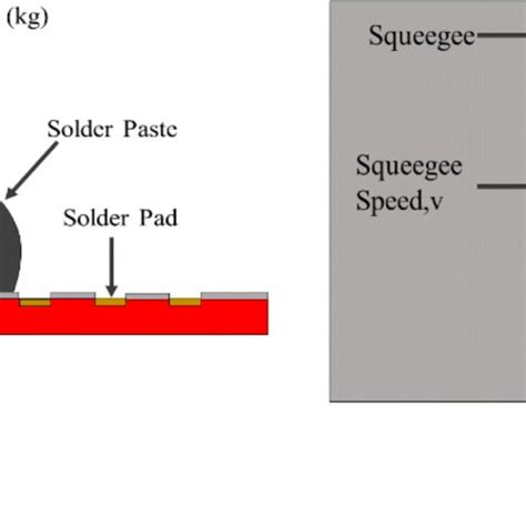
Printer settings: The print speed, pressure, and separation distance must be adjusted to achieve the desired solder paste deposit volume and shape.
-
PCB surface finish: The PCB surface finish, such as HASL, ENIG, or OSP, can affect the solder paste’s wetting and spreading behavior.
-
Environmental conditions: Temperature, humidity, and airborne contaminants can affect the solder paste’s rheology and printing performance.
By understanding and controlling these factors, engineers can optimize the solder paste printing process and achieve high-quality solder joints.

Tips for Optimizing Solder Paste Printing
1. Stencil Design Optimization
The stencil is the most critical component in the solder paste printing process. It determines the amount and distribution of solder paste deposited onto the PCB pads. To optimize the stencil design, consider the following:
-
Aperture size: The aperture size should be slightly larger than the PCB pad size to allow for some solder paste shrinkage during reflow. A typical oversize is 10-20% of the pad size.
-
Aperture shape: The aperture shape should match the pad shape to ensure even solder paste distribution. For example, use rectangular apertures for rectangular pads and circular apertures for circular pads.
-
Stencil thickness: The stencil thickness should be selected based on the desired solder paste volume and the component pitch. Thinner stencils (100-150 μm) are suitable for fine-pitch components, while thicker stencils (150-200 μm) are better for larger components.
-
Aperture wall angle: The aperture wall angle should be between 5-15° to facilitate solder paste release from the stencil. Larger angles can cause solder paste slumping, while smaller angles can cause solder paste sticking.
| Component Pitch | Recommended Stencil Thickness |
|---|---|
| < 0.5 mm | 100-120 μm |
| 0.5-0.8 mm | 120-150 μm |
| > 0.8 mm | 150-200 μm |
2. Solder Paste Selection
Selecting the right solder paste for the application is crucial for achieving good printing performance and solder joint quality. Consider the following factors when selecting a solder paste:
-
Alloy composition: The most common solder paste alloys are Sn-Pb (e.g., Sn63Pb37) and lead-free (e.g., SAC305). Lead-free alloys generally require higher reflow temperatures and have different wetting and spreading behaviors compared to Sn-Pb alloys.
-
Particle size: Solder paste particle size is classified by mesh size, with larger numbers indicating smaller particles. Fine-pitch applications typically require smaller particle sizes (Type 4 or higher) to prevent bridging, while larger components can use larger particle sizes (Type 3).
-
Flux activity: The flux in the solder paste serves to remove oxides from the metal surfaces and promote solder wetting. Flux activity is classified as low (L), medium (M), or high (H). Higher activity fluxes are better for hard-to-solder surfaces, but they also require more thorough cleaning after reflow.
-
Viscosity: Solder paste viscosity affects its printability and slump resistance. Higher viscosity pastes are better for fine-pitch applications and stencils with smaller apertures, while lower viscosity pastes are better for larger components and thicker stencils.
| Solder Paste Type | Particle Size (μm) | Mesh Size |
|---|---|---|
| Type 3 | 25-45 | -325/+500 |
| Type 4 | 20-38 | -400/+635 |
| Type 5 | 15-25 | -500/+800 |
| Type 6 | 5-15 | -635 |
3. Printer Setup and Maintenance
Proper printer setup and maintenance are essential for consistent solder paste printing quality. Consider the following tips:
-
Print speed: The print speed should be adjusted based on the solder paste viscosity and the stencil aperture size. Higher viscosity pastes and smaller apertures require slower print speeds to allow enough time for the paste to fill the apertures. A typical print speed range is 20-100 mm/s.
-
Print pressure: The print pressure should be sufficient to force the solder paste through the stencil apertures and onto the PCB pads, but not so high as to cause solder paste bleeding or stencil damage. A typical print pressure range is 0.2-0.6 kg/cm².
-
Separation distance: The separation distance between the stencil and the PCB should be minimized to prevent solder paste slumping and bridging. A typical separation distance is 0.1-0.3 mm.
-
Stencil cleaning: The stencil should be cleaned regularly to remove solder paste residue and prevent aperture clogging. Use a compatible solvent and a lint-free wipe or brush to avoid damaging the stencil surface.
-
Printer calibration: The printer should be calibrated periodically to ensure accurate stencil-to-PCB alignment and consistent print results. Follow the manufacturer’s recommended calibration procedure and frequency.
4. Process Control and Monitoring
Implementing process control and monitoring techniques can help identify and correct solder paste printing issues before they affect product quality. Consider the following:
-
Solder paste inspection (SPI): SPI systems use 2D or 3D imaging to measure the volume, height, and area of solder paste deposits on the PCB. SPI data can be used to detect printing defects, such as insufficient or excessive solder paste, bridging, or missing deposits.
-
Statistical process control (SPC): SPC involves collecting and analyzing process data over time to identify trends and variations. Control charts can be used to monitor key printing parameters, such as paste volume, height, and area, and to set control limits for acceptable performance.
-
Design of experiments (DOE): DOE is a structured approach to optimizing process parameters by systematically varying them and measuring their effects on output variables. DOE can be used to identify the most critical printing parameters and their optimal settings for a given PCB design and solder paste.
-
Operator training: Operators should be trained on proper solder paste handling, printer setup, and stencil cleaning procedures to ensure consistent printing quality. Visual aids, such as defect reference images and process control charts, can help operators identify and correct printing issues.

Frequently Asked Questions
1. What is the shelf life of solder paste, and how should it be stored?
The shelf life of solder paste depends on the specific product and its storage conditions. Most solder pastes have a shelf life of 6-12 months when stored at 0-10°C in an airtight container. Solder paste should be allowed to reach room temperature before use, and any expired or contaminated paste should be discarded.
2. Can solder paste be reused after printing?
Solder paste that has been printed through a stencil cannot be reused due to the risk of contamination and changes in rheology. Any excess solder paste should be discarded after printing. However, unused solder paste that has been properly stored in an airtight container can be used for future printing jobs.
3. How do I choose the right solder paste for my application?
Choosing the right solder paste depends on several factors, including the PCB design, component types, and reflow profile. Consider the following guidelines:
- For fine-pitch components (< 0.5 mm pitch), use a Type 4 or higher solder paste with a compatible particle size and viscosity.
- For larger components (> 0.8 mm pitch), use a Type 3 solder paste with a compatible flux activity and alloy composition.
- For lead-free applications, use a SAC alloy paste with a higher reflow temperature and a compatible flux activity.
- For hard-to-solder surfaces, such as OSP or oxidized pads, use a higher activity flux (RMA or RS).
Consult with your solder paste supplier or assembly service provider for specific recommendations based on your application requirements.
4. What are some common solder paste printing defects, and how can they be prevented?
Some common solder paste printing defects include:
-
Insufficient solder paste: Caused by clogged stencil apertures, low print pressure, or high print speed. Prevent by cleaning the stencil regularly, increasing print pressure, and reducing print speed.
-
Excessive solder paste: Caused by oversized stencil apertures, high print pressure, or low print speed. Prevent by optimizing stencil aperture size, reducing print pressure, and increasing print speed.
-
Solder bridging: Caused by excessive solder paste, slumping, or stencil misalignment. Prevent by optimizing stencil aperture size and shape, reducing separation distance, and improving stencil-to-PCB alignment.
-
Solder balls: Caused by solder paste contamination, excessive flux activity, or incompatible reflow profile. Prevent by using fresh solder paste, selecting a compatible flux activity, and optimizing the reflow profile.
5. How often should I clean my stencil, and what cleaning methods are recommended?
Stencil cleaning frequency depends on the solder paste type, printing volume, and environmental conditions. As a general guideline, clean the stencil every 4-8 hours of continuous printing, or whenever print quality starts to degrade.
Recommended stencil cleaning methods include:
-
Manual cleaning: Use a compatible solvent (e.g., isopropyl alcohol) and a lint-free wipe or brush to remove solder paste residue from the stencil surface and apertures.
-
Automated cleaning: Use an inline or offline stencil cleaning system with a compatible cleaning agent and brushes or ultrasonic nozzles to remove solder paste residue.
-
Dry cleaning: Use a vacuum system with micro-abrasive particles to remove solder paste residue without the need for solvents.
Always follow the manufacturer’s recommended cleaning procedure and frequency for your specific stencil and solder paste type to ensure optimal printing performance and stencil life.
Conclusion
Solder paste printing is a critical step in the SMT assembly process that directly affects the quality and reliability of the final product. By understanding the factors affecting solder paste printing quality and implementing best practices for stencil design, solder paste selection, printer setup, and process control, engineers can optimize the printing process and achieve high-quality solder joints.
Some key tips for optimizing solder paste printing include:
- Optimizing stencil aperture size, shape, and thickness for the specific PCB design and solder paste properties.
- Selecting a solder paste with compatible alloy composition, particle size, flux activity, and viscosity for the application.
- Setting up the printer with appropriate print speed, pressure, and separation distance, and maintaining it with regular stencil cleaning and calibration.
- Implementing process control and monitoring techniques, such as SPI, SPC, and DOE, to identify and correct printing issues.
By following these tips and continuously improving the solder paste printing process, manufacturers can reduce defects, increase yields, and improve the overall quality and reliability of their SMT assemblies.


Leave a Reply