Introduction to Via Fill PCB Technology
In the world of printed circuit board (PCB) manufacturing, via fill technology has become increasingly important as electronic devices continue to shrink in size while demanding higher performance. Via fill PCB technology involves filling the drilled holes (vias) in a PCB with a conductive or non-conductive material to enhance the board’s electrical, thermal, and mechanical properties. This article will explore the differences between conductive and non-conductive via fill PCB, their applications, advantages, and disadvantages, as well as the various methods used to fill vias.
What is a Via?
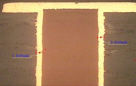
Before diving into via fill technology, it’s essential to understand what a via is. A via is a small hole drilled through a PCB to connect different layers of the board electrically. Vias allow signals to travel from one layer to another, enabling more complex circuit designs and reducing the overall size of the PCB.
Types of Vias
There are several types of vias used in PCB design, each serving a specific purpose:
-
Through-hole vias: These vias extend through all layers of the PCB and are typically used for mounting through-hole components or providing structural support.
-
Blind vias: These vias connect an outer layer to an inner layer without extending through the entire board thickness.
-
Buried vias: These vias connect inner layers without extending to either outer layer of the PCB.
-
Micro vias: These are small vias (typically less than 150 microns in diameter) used for high-density interconnect (HDI) PCB designs.
Conductive Via Fill PCB
Conductive via fill PCB technology involves filling the vias with a conductive material, such as copper or silver epoxy. This process creates a solid, electrically conductive connection between the layers of the PCB, offering several advantages over unfilled vias.
Advantages of Conductive Via Fill
-
Improved electrical performance: Conductive via fill reduces the inductance and resistance of the vias, allowing for faster signal transmission and reducing signal loss. This is particularly important for high-speed digital circuits and RF applications.
-
Enhanced thermal management: Conductive via fill improves the thermal conductivity of the PCB, allowing heat to dissipate more efficiently from high-power components. This can help prevent overheating and improve the overall reliability of the electronic device.
-
Increased mechanical strength: Filled vias provide additional structural support to the PCB, reducing the risk of via cracking or delamination during the assembly process or in harsh operating environments.
-
Better manufacturability: Conductive via fill allows for the creation of landless vias, which can be placed directly under components, saving space on the PCB and enabling higher-density designs.
Disadvantages of Conductive Via Fill
-
Higher cost: The process of filling vias with conductive material adds an additional step to the PCB manufacturing process, increasing the overall cost of the board.
-
Longer production time: Conductive via fill requires additional processing time, which can lengthen the overall production timeline for the PCB.
-
Potential for voiding: If the via fill process is not properly controlled, voids or air pockets can form within the filled via, potentially reducing its electrical and thermal performance.
Applications of Conductive Via Fill PCB
Conductive via fill PCB technology is commonly used in applications that require high electrical performance, thermal management, or mechanical stability, such as:
- High-speed digital circuits (e.g., CPUs, GPUs, ASICs)
- RF and microwave devices (e.g., antennas, filters, amplifiers)
- Power electronics (e.g., motor drives, power supplies, inverters)
- Automotive and aerospace electronics
- Medical devices

Non-Conductive Via Fill PCB
Non-conductive via fill PCB technology involves filling the vias with a non-conductive material, such as epoxy resin. This process is typically used to improve the mechanical and thermal properties of the PCB without affecting its electrical performance.
Advantages of Non-Conductive Via Fill
-
Improved thermal management: Non-conductive via fill can help dissipate heat from high-power components by providing a thermal path through the PCB, reducing the risk of overheating and improving the device’s reliability.
-
Enhanced mechanical strength: Filled vias provide additional structural support to the PCB, reducing the risk of via cracking or delamination during the assembly process or in harsh operating environments.
-
Reduced capacitive coupling: Non-conductive via fill can help reduce capacitive coupling between adjacent vias or traces, improving the signal integrity of the PCB.
-
Lower cost compared to conductive via fill: Non-conductive via fill is generally less expensive than conductive via fill, as the materials used are more readily available and the process is less complex.
Disadvantages of Non-Conductive Via Fill
-
No electrical connectivity: Non-conductive via fill does not provide electrical connectivity between layers, so additional vias may be required for signal routing.
-
Potential for CTE mismatch: If the coefficient of thermal expansion (CTE) of the non-conductive fill material differs significantly from that of the PCB substrate, thermal stresses can develop, potentially causing reliability issues.
Applications of Non-Conductive Via Fill PCB
Non-conductive via fill PCB technology is commonly used in applications that require improved thermal management or mechanical stability without the need for enhanced electrical performance, such as:
- High-power LED lighting
- Automotive and aerospace electronics
- Industrial control systems
- Consumer electronics

Via Fill Methods
There are several methods used to fill vias in PCB manufacturing, each with its own advantages and disadvantages. The choice of method depends on the specific requirements of the application, the materials used, and the available manufacturing capabilities.
Screen Printing
Screen printing is a common method for filling vias with conductive or non-conductive materials. In this process, a stencil is placed over the PCB, and the fill material is pushed through the stencil openings into the vias using a squeegee. The excess material is then removed, and the PCB is cured to harden the fill material.
| Advantages | Disadvantages |
|---|---|
| Cost-effective for large volumes | Limited to larger Via sizes |
| High throughput | Potential for voiding |
| Suitable for both conductive and non-conductive fill materials | Requires additional curing step |
Vacuum Plating
Vacuum plating is a method used for filling vias with conductive materials, such as copper. In this process, the PCB is placed in a vacuum chamber, and a conductive seed layer is deposited onto the via walls using physical vapor deposition (PVD) or electroless plating. The vias are then filled with copper using electroplating.
| Advantages | Disadvantages |
|---|---|
| Provides complete via fill | Higher cost compared to other methods |
| Suitable for small via sizes | Longer processing time |
| Excellent electrical conductivity | Limited to conductive fill materials |
Electroplating
Electroplating is another method used for filling vias with conductive materials. In this process, the PCB is immersed in an electrolytic solution, and an electric current is applied to deposit the conductive material onto the via walls and fill the vias.
| Advantages | Disadvantages |
|---|---|
| Provides complete via fill | Requires conductive seed layer |
| Suitable for small via sizes | Potential for voiding |
| Good electrical conductivity | Limited to conductive fill materials |
Conductive Paste Filling
Conductive paste filling involves dispensing a conductive paste, such as silver-filled epoxy, into the vias using a syringe or a paste dispenser. The PCB is then cured to harden the fill material.
| Advantages | Disadvantages |
|---|---|
| Cost-effective for small volumes | Limited to larger via sizes |
| Suitable for prototype and low-volume production | Potential for voiding |
| Can be used for both conductive and non-conductive fill materials | Lower electrical conductivity compared to plating methods |

Designing for Via Fill PCB
When designing a PCB that will use via fill technology, several factors must be considered to ensure the best performance and manufacturability:
-
Via size and aspect ratio: The via size and aspect ratio (depth-to-diameter ratio) should be compatible with the chosen via fill method. Smaller vias and higher aspect ratios may require specialized fill methods or materials.
-
Via location and spacing: Vias should be placed in locations that allow for proper filling and minimize the risk of voiding. Adequate spacing between vias should be maintained to prevent shorting or other manufacturing defects.
-
Material selection: The choice of fill material should be based on the specific requirements of the application, such as electrical conductivity, thermal conductivity, and CTE compatibility with the PCB substrate.
-
Manufacturing capabilities: The design should take into account the available manufacturing capabilities and limitations of the PCB fabricator, such as minimum via size, aspect ratio, and fill methods.
Conclusion
Conductive and non-conductive via fill PCB technologies offer unique advantages and disadvantages for various applications. Conductive via fill provides improved electrical performance, thermal management, and mechanical strength, making it suitable for high-speed digital circuits, RF devices, and power electronics. Non-conductive via fill, on the other hand, offers enhanced thermal management and mechanical stability without affecting electrical performance, making it suitable for applications such as LED lighting and consumer electronics.
The choice between conductive and non-conductive via fill depends on the specific requirements of the application, the materials used, and the available manufacturing capabilities. By understanding the differences between these technologies and the various via fill methods, designers can create PCBs that meet the demanding requirements of modern electronic devices while optimizing performance, reliability, and cost.
Frequently Asked Questions (FAQ)
-
What is the difference between conductive and non-conductive via fill?
Conductive via fill involves filling the vias with a conductive material, such as copper or silver epoxy, creating an electrical connection between layers. Non-conductive via fill uses a non-conductive material, such as epoxy resin, to improve the mechanical and thermal properties of the PCB without affecting its electrical performance. -
What are the advantages of using via fill technology in PCB design?
Via fill technology offers several advantages, including improved electrical performance, enhanced thermal management, increased mechanical strength, better manufacturability, and reduced capacitive coupling, depending on whether conductive or non-conductive fill materials are used. -
What are the common methods used for filling vias in PCB manufacturing?
Common via fill methods include screen printing, vacuum plating, electroplating, and conductive paste filling. Each method has its own advantages and disadvantages, and the choice of method depends on the specific requirements of the application, the materials used, and the available manufacturing capabilities. -
How does via fill technology affect the cost and production time of a PCB?
Via fill technology, particularly conductive via fill, can increase the cost and production time of a PCB due to the additional processing steps required. However, the benefits of via fill, such as improved performance and reliability, often outweigh the increased cost and production time for certain applications. -
What factors should be considered when designing a PCB that will use via fill technology?
When designing a PCB that will use via fill technology, factors such as via size and aspect ratio, via location and spacing, material selection, and manufacturing capabilities should be considered to ensure the best performance and manufacturability of the board.


Leave a Reply