Introduction to PCB Inkjet Printing
Printed Circuit Boards (PCBs) are essential components in modern electronics. They provide a platform for mounting and connecting electronic components, allowing for the creation of complex circuits. Traditionally, PCBs are manufactured using a subtractive process, where copper is selectively removed from a substrate to create the desired circuit pattern. However, recent advancements in inkjet printing technology have opened up new possibilities for PCB production.
Inkjet printing offers several advantages over traditional PCB manufacturing methods. It is a non-contact, additive process that allows for the precise deposition of conductive and insulating materials onto a substrate. This enables the creation of highly customized and complex circuit designs with ease. Additionally, inkjet printing is cost-effective for low-volume production and prototyping, as it eliminates the need for expensive tooling and setup costs.
In this article, we will explore the process of modding an inkjet printer for PCB production. We will cover the necessary hardware and software modifications, the materials and inks used, and the steps involved in printing a functional PCB using an inkjet printer.
Hardware Modifications for PCB Inkjet Printing
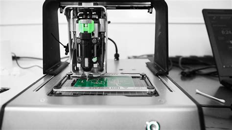
To use an inkjet printer for PCB production, several hardware modifications are required. These modifications ensure that the printer can handle the specialized inks and substrates used in the process.
Printhead and Ink Cartridges
The first step in modding an inkjet printer for PCB production is to replace the standard ink cartridges with ones that are compatible with conductive and insulating inks. These inks have different properties compared to regular printer inks, such as higher viscosity and particle size. It is important to select cartridges that are specifically designed for use with these specialized inks to ensure optimal performance and prevent clogging.
In addition to the ink cartridges, the printhead may also require modification. Some inkjet printers use thermal printheads, which heat the ink to create droplets. However, conductive inks may not be suitable for use with thermal printheads due to their high viscosity and potential for clogging. In such cases, it may be necessary to replace the thermal printhead with a piezoelectric printhead, which uses mechanical pressure to create droplets.
Substrate Handling and Alignment
Another important hardware modification involves the substrate handling and alignment system. PCBs require precise alignment and registration to ensure that the printed circuit pattern matches the desired design. This can be achieved by modifying the printer’s paper feed mechanism to accommodate the thicker and more rigid substrates used in PCB production.
One common approach is to replace the standard paper feed rollers with a vacuum table or a flatbed system. A vacuum table uses suction to hold the substrate in place, while a flatbed system uses a flat surface with alignment pins or guides to ensure accurate positioning. These modifications allow for the precise and repeatable alignment of the substrate, which is crucial for achieving high-quality PCB prints.
Curing and Sintering Equipment
After printing the circuit pattern onto the substrate, the conductive ink needs to be cured and sintered to achieve optimal electrical conductivity. This process involves exposing the printed ink to heat or other energy sources to remove any solvents and fuse the conductive particles together.
To facilitate this process, additional equipment may need to be integrated into the printer setup. This can include a heating element, such as an infrared lamp or a hot air gun, to provide the necessary heat for curing and sintering. Alternatively, some setups may use photonic sintering, which involves exposing the printed ink to intense light pulses to achieve rapid sintering.

Software Modifications for PCB Inkjet Printing
In addition to hardware modifications, software changes are also necessary to enable an inkjet printer to produce PCBs. These modifications involve the printer driver, the CAD/CAM software, and the print settings.
Printer Driver Modifications
The printer driver is responsible for translating the digital image data into instructions for the printer hardware. To use an inkjet printer for PCB production, the driver needs to be modified to support the specialized inks and substrates used in the process.
This may involve adjusting the drop size, firing frequency, and other parameters to optimize the performance of the conductive and insulating inks. Additionally, the driver may need to be configured to handle the different color channels used for the various inks, such as silver for conductive traces and dielectric for insulating layers.
CAD/CAM Software Integration
To design and prepare the PCB layout for printing, CAD (Computer-Aided Design) and CAM (Computer-Aided Manufacturing) software is used. These tools allow for the creation of the circuit schematic, the component placement, and the generation of the final print files.
To integrate the CAD/CAM software with the modified inkjet printer, additional plugins or scripts may be required. These plugins handle tasks such as generating the appropriate print files, compensating for any distortions or shrinkage in the printed pattern, and optimizing the print settings for the specific ink and substrate combination.
Print Settings Optimization
The print settings play a crucial role in achieving high-quality PCB prints. These settings include the resolution, the number of layers, the ink droplet size, and the curing/sintering parameters.
Optimization of these settings involves experimentation and fine-tuning to find the ideal combination for the specific ink and substrate being used. Factors such as the ink viscosity, the substrate surface energy, and the desired feature size and resolution all need to be considered when determining the optimal print settings.

Materials and Inks for PCB Inkjet Printing
The materials and inks used in PCB inkjet printing are specialized and designed to meet the unique requirements of the process. These include the substrates, the conductive inks, and the insulating inks.
Substrates for PCB Inkjet Printing
The substrate is the base material onto which the circuit pattern is printed. Common substrates used in PCB inkjet printing include:
- FR-4: A glass-reinforced epoxy laminate that is widely used in traditional PCB manufacturing. It offers good mechanical and electrical properties and is compatible with inkjet printing.
- Polyimide: A flexible plastic material that is suitable for creating flexible PCBs. It has excellent thermal and chemical resistance and can withstand the high temperatures used in the curing and sintering process.
- Paper: Low-cost, eco-friendly option for disposable or single-use PCBs. It is biodegradable and can be easily printed on using inkjet technology.
| Substrate | Advantages | Disadvantages |
|---|---|---|
| FR-4 | – Good mechanical and electrical properties – Wide availability – Compatibility with traditional PCB processes |
– Rigid and inflexible – Higher cost compared to paper |
| Polyimide | – Flexibility – High thermal and chemical resistance – Suitable for wearable and bendable electronics |
– Higher cost compared to FR-4 and paper – May require specialized handling and processing |
| Paper | – Low cost – Eco-friendly and biodegradable – Suitable for disposable and single-use applications |
– Limited mechanical and electrical properties – Susceptible to moisture and environmental factors |
Conductive Inks for PCB Inkjet Printing
Conductive inks are used to print the conductive traces and pads on the PCB. These inks typically contain metal nanoparticles, such as silver or copper, dispersed in a solvent. When printed and cured, the metal particles fuse together to form a continuous conductive path.
Some common conductive inks used in PCB inkjet printing include:
- Silver nanoparticle ink: Offers high conductivity and compatibility with a wide range of substrates. It is the most widely used conductive ink in PCB inkjet printing.
- Copper nanoparticle ink: Provides a lower-cost alternative to silver ink while still offering good conductivity. However, it may require a more complex sintering process to achieve optimal performance.
- Conductive polymer ink: Uses intrinsically conductive polymers instead of metal nanoparticles. These inks offer the potential for lower cost and greater flexibility compared to metal-based inks.
Insulating Inks for PCB Inkjet Printing
Insulating inks, also known as dielectric inks, are used to create insulating layers between conductive traces on the PCB. These inks are typically polymers or ceramic materials that provide electrical insulation and protection against short circuits.
Some common insulating inks used in PCB inkjet printing include:
- UV-curable polymer ink: Uses ultraviolet (UV) light to cure and harden the insulating layer. It offers good dielectric properties and can be quickly cured using a UV lamp.
- Thermal-curable polymer ink: Requires heat to cure and form the insulating layer. It provides good thermal and mechanical stability and is suitable for high-temperature applications.
- Ceramic ink: Uses ceramic particles dispersed in a polymer matrix to create a high-performance insulating layer. It offers excellent dielectric properties and thermal stability, making it suitable for demanding applications.

The PCB Inkjet Printing Process
The process of printing a PCB using an inkjet printer involves several steps, from design to final curing and sintering. Here is an overview of the key stages in the PCB inkjet printing process:
-
PCB Design: The first step is to create the PCB layout using CAD software. This involves designing the circuit schematic, placing the components, and generating the final print files.
-
Substrate Preparation: The chosen substrate is loaded into the modified inkjet printer and aligned using the substrate handling and alignment system. The substrate surface may need to be cleaned or treated to ensure good ink adhesion.
-
Printing: The modified inkjet printer deposits the conductive and insulating inks onto the substrate according to the PCB design. The printing process is typically carried out in multiple passes, with each pass laying down a specific layer of ink.
-
Drying: After each printing pass, the deposited ink is allowed to dry. This can be done using ambient air or by using a drying system, such as a heated bed or an infrared lamp.
-
Insulating Layer Printing: If the PCB design requires insulating layers, these are printed using the insulating ink. The insulating layers are deposited between the conductive layers to prevent short circuits and provide electrical isolation.
-
Curing and Sintering: Once all the layers have been printed and dried, the PCB undergoes a curing and sintering process. This involves exposing the printed inks to heat or other energy sources to remove any remaining solvents and fuse the conductive particles together. The specific curing and sintering parameters depend on the type of ink used and the desired electrical and mechanical properties of the final PCB.
-
Post-Processing: After curing and sintering, the PCB may require additional post-processing steps, such as drilling holes for through-hole components, applying solder mask, or adding surface finishes. These steps can be performed using traditional PCB manufacturing techniques or by using specialized inkjet printing processes.
-
Quality Control: Finally, the printed PCB undergoes quality control checks to ensure that it meets the desired specifications and performance requirements. This may involve visual inspection, electrical testing, and other quality assurance measures.
Advantages and Limitations of PCB Inkjet Printing
PCB inkjet printing offers several advantages over traditional PCB manufacturing methods, but it also has some limitations. Here are some of the key advantages and limitations of PCB inkjet printing:
Advantages
-
Rapid Prototyping: Inkjet printing allows for quick and easy prototyping of PCB designs. Designs can be easily modified and reprinted, enabling faster iteration and optimization of the PCB layout.
-
Cost-Effective for Low Volumes: For low-volume production and prototyping, inkjet printing is more cost-effective compared to traditional PCB manufacturing methods. It eliminates the need for expensive tooling and setup costs associated with subtractive processes like etching.
-
High Customization: Inkjet printing enables the creation of highly customized PCB designs. Complex shapes, fine features, and non-standard layouts can be easily printed, offering greater design flexibility compared to traditional methods.
-
Environmentally Friendly: Inkjet printing is an additive process, meaning that it only deposits material where needed. This reduces waste compared to subtractive processes, which remove material to create the circuit pattern. Additionally, some of the inks and substrates used in inkjet printing are eco-friendly and biodegradable.
Limitations
-
Limited Material Selection: The range of materials and inks available for PCB inkjet printing is currently limited compared to traditional PCB manufacturing. Some high-performance materials, such as low-loss dielectrics or high-temperature substrates, may not be readily available or compatible with inkjet printing.
-
Lower Resolution and Feature Size: Inkjet printing typically has lower resolution and larger minimum feature sizes compared to traditional PCB manufacturing methods. This limitation is due to the size of the ink droplets and the spreading of the ink on the substrate surface. As a result, inkjet printing may not be suitable for applications requiring very fine pitch or high-density interconnects.
-
Slower Production Speed: Compared to large-scale PCB manufacturing methods, such as screen printing or photolithography, inkjet printing has a slower production speed. This is because the printing process is carried out in multiple passes, and each layer needs to be dried and cured before the next layer can be printed. As a result, inkjet printing may not be suitable for high-volume production.
-
Ink Formulation Challenges: Developing and optimizing ink formulations for PCB inkjet printing can be challenging. The inks need to have suitable rheological properties, such as viscosity and surface tension, to ensure reliable jetting and droplet formation. Additionally, the inks need to have good adhesion to the substrate, high conductivity, and compatibility with the curing and sintering processes.
Frequently Asked Questions (FAQ)
- What types of inkjet printers can be used for PCB printing?
-
Most consumer-grade inkjet printers can be modified for PCB printing, including those from brands like Epson, Canon, and HP. However, some models may be more suitable than others due to their printhead technology, ink compatibility, and ease of modification.
-
Can I use regular printer ink for PCB printing?
-
No, regular printer ink cannot be used for PCB printing. PCB printing requires specialized conductive and insulating inks that have different properties compared to standard printer inks. These specialized inks are designed to provide the necessary electrical conductivity and insulation for the printed circuit board.
-
What is the minimum feature size achievable with PCB inkjet printing?
-
The minimum feature size achievable with PCB inkjet printing depends on several factors, such as the printer resolution, ink droplet size, and substrate properties. Typically, PCB inkjet printing can achieve feature sizes down to around 50-100 microns (μm). However, more advanced systems and optimized ink formulations may enable smaller feature sizes.
-
How long does it take to print a PCB using an inkjet printer?
-
The printing time for a PCB using an inkjet printer varies depending on the size and complexity of the design, as well as the specific printer and ink settings used. A simple, single-layer PCB may take a few minutes to print, while a more complex, multi-layer PCB may take several hours. Additionally, the drying, curing, and sintering processes can add significant time to the overall production process.
-
Can I use inkjet printing for mass production of PCBs?
- Inkjet printing is generally not suitable for mass production of PCBs due to its slower production speed compared to traditional manufacturing methods. However, it is well-suited for prototyping, low-volume production, and customized PCB designs. For high-volume production, methods like screen printing or photolithography are typically more efficient and cost-effective.
Conclusion
PCB inkjet printing is a promising technology that offers several advantages over traditional PCB manufacturing methods. By modding an inkjet printer and using specialized inks and substrates, it is possible to create highly customized and complex PCB designs with ease. Inkjet printing enables rapid prototyping, cost-effective low-volume production, and greater design flexibility compared to subtractive processes.
However, PCB inkjet printing also has some limitations, such as limited material selection, lower resolution and feature size, slower production speed, and ink formulation challenges. Despite these limitations, the technology continues to evolve and improve, with ongoing research and development efforts aimed at enhancing the capabilities and performance of PCB inkjet printing.
As the demand for customized and low-volume PCB production grows, particularly in fields like wearable electronics, Internet of Things (IoT) devices, and flexible electronics, PCB inkjet printing is likely to play an increasingly important role. By enabling rapid prototyping and cost-effective production of complex PCB designs, inkjet printing opens up new possibilities for innovation and product development in the electronics industry.
In conclusion, PCB inkjet printing is a powerful tool for those looking to create custom PCBs quickly and efficiently. By understanding the hardware and software modifications required, the materials and inks used, and the printing process itself, anyone can start exploring the potential of this exciting technology. As PCB inkjet printing continues to evolve, it is poised to revolutionize the way we design and manufacture electronic devices in the future.


Leave a Reply