Introduction to PCB Design and KiCad
Printed Circuit Boards (PCBs) are the backbone of modern electronics. They provide a platform for electronic components to be mounted and interconnected, enabling the creation of complex circuits and devices. Designing a PCB can be a daunting task, especially for beginners. However, with the right tools and knowledge, anyone can create a professional-quality PCB.
One of the most popular and powerful tools for PCB design is KiCad. KiCad is a free, open-source software suite that provides a complete set of tools for designing electronic circuits and creating PCBs. In this article, we will guide you through the process of creating a PCB using KiCad, from schematic design to PCB layout and fabrication.
What is KiCad?
KiCad is a cross-platform, open-source software suite for Electronic Design Automation (EDA). It provides a set of tools for designing electronic circuits and creating PCBs, including:
- Eeschema: A schematic capture editor for creating circuit diagrams
- Pcbnew: A PCB layout editor for designing the physical layout of the PCB
- GerbView: A Gerber file viewer for inspecting the output files for PCB fabrication
- Bitmap2Component: A tool for converting images into footprints for PCB components
- PCB Calculator: A tool for calculating various PCB parameters, such as trace width and impedance
KiCad is available for Windows, macOS, and Linux, and it supports a wide range of file formats for importing and exporting designs.
Why Use KiCad for PCB Design?
There are many reasons why KiCad is a popular choice for PCB design, including:
- It’s free and open-source, which means anyone can use it without paying for expensive licenses
- It’s cross-platform, which means it can be used on any operating system
- It has a large and active community of users and developers who provide support, tutorials, and resources
- It supports a wide range of file formats, making it easy to integrate with other tools and services
- It provides a complete set of tools for designing electronic circuits and creating PCBs, from schematic capture to PCB layout and fabrication
Getting Started with KiCad
Installing KiCad
Before we can start designing our PCB, we need to install KiCad on our computer. KiCad is available for download from the official website: https://www.kicad.org/download/
Choose the appropriate version for your operating system and follow the installation instructions. Once the installation is complete, launch KiCad from the application menu or desktop shortcut.
Creating a New Project
When you launch KiCad for the first time, you will be presented with the main window, which provides access to all the tools and functions of the software. To create a new project, click on the “File” menu and select “New Project.”
Choose a location for your project and give it a name. KiCad will create a new project folder with the necessary files and directories.
Creating a Schematic
The first step in designing a PCB is to create a schematic diagram of the circuit. A schematic is a graphical representation of the electronic components and their interconnections. To create a schematic in KiCad, we will use the Eeschema tool.
From the main KiCad window, click on the “Eeschema” button to launch the schematic editor. You will be presented with a blank schematic sheet, ready for you to start adding components and connections.
Adding Components
To add a component to the schematic, click on the “Place” button in the toolbar and select “Component.” This will open the component library browser, where you can search for and select the component you want to add.
Once you have selected a component, click on the schematic sheet to place it. You can move and rotate the component using the mouse or the arrow keys on the keyboard.
Repeat this process for all the components in your circuit. Be sure to give each component a unique reference designator (e.g. R1, C1, U1) to identify it in the schematic and PCB layout.
Adding Connections
Once you have placed all the components on the schematic sheet, you need to connect them together using wires. To add a wire, click on the “Place” button in the toolbar and select “Wire.”
Click on the first component pin you want to connect, then click on the second pin to complete the connection. KiCad will automatically route the wire between the two pins.
Repeat this process for all the connections in your circuit. Be sure to use labels and net names to identify important signals and power nets.
Adding Power and Ground Symbols
Most circuits require power and ground connections. To add these to your schematic, click on the “Place” button in the toolbar and select “Power Port.”
Choose the appropriate power or ground symbol from the library and place it on the schematic sheet. Connect the power and ground symbols to the appropriate component pins using wires.
Checking the Schematic
Once you have completed your schematic, it’s a good idea to check it for errors and inconsistencies. KiCad provides a built-in Electrical Rules Check (ERC) tool that can help you identify potential problems with your schematic.
To run the ERC, click on the “Tools” menu and select “Electrical Rules Check.” KiCad will analyze your schematic and report any errors or warnings in the Messages panel at the bottom of the window.
Review the errors and warnings and make any necessary corrections to your schematic. Once you are satisfied that your schematic is correct, you can move on to the PCB layout phase.
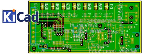
Creating a PCB Layout
With your schematic complete, you are now ready to create the physical layout of your PCB. To do this, we will use the Pcbnew tool in KiCad.
From the main KiCad window, click on the “Pcbnew” button to launch the PCB layout editor. You will be presented with a blank PCB sheet, ready for you to start placing components and routing traces.
Importing the Netlist
The first step in creating a PCB layout is to import the netlist from your schematic. The netlist is a file that contains information about the components and connections in your circuit.
To import the netlist, click on the “Tools” menu and select “Update PCB from Schematic.” KiCad will read the netlist from your schematic and populate the PCB layout with the appropriate components and connections.
Placing Components
With the netlist imported, you can now start placing components on the PCB. To place a component, click on the “Place” button in the toolbar and select “Footprint.”
Choose the appropriate footprint for each component from the library and place it on the PCB. You can move and rotate the footprint using the mouse or the arrow keys on the keyboard.
Be sure to consider the placement of components carefully, taking into account factors such as signal integrity, thermal management, and mechanical constraints.
Routing Traces
Once you have placed all the components on the PCB, you need to route the traces that connect them together. To route a trace, click on the “Route” button in the toolbar and select “Track.”
Click on the first pad you want to connect, then click on the second pad to complete the connection. KiCad will automatically route the trace between the two pads, avoiding obstacles and following the design rules you have specified.
Repeat this process for all the connections in your circuit. Be sure to use appropriate trace widths and spacings for each signal, based on factors such as current, voltage, and frequency.
Adding Copper Pours
Copper pours are large areas of copper on the PCB that are used for power and ground planes, as well as for shielding and thermal management. To add a copper pour, click on the “Place” button in the toolbar and select “Copper Pour.”
Choose the appropriate layer for the copper pour (e.g. Front Copper, Back Copper) and draw a polygon around the area you want to fill with copper. KiCad will automatically fill the area with copper, connecting it to any pads or traces that overlap with it.
Adding Silkscreen and Solder Mask
Silkscreen and solder mask are two important layers that are used for labeling and protecting the PCB. Silkscreen is used for adding text and graphics to the PCB, while solder mask is used for covering the copper areas that should not be exposed to solder during the assembly process.
To add silkscreen and solder mask, click on the “Layers” button in the toolbar and select the appropriate layer (e.g. Front Silkscreen, Back Solder Mask). Use the drawing tools to add text, graphics, and shapes to the layer.
Be sure to follow the design rules for silkscreen and solder mask, such as minimum clearances and apertures.
Checking the PCB Layout
Once you have completed your PCB layout, it’s a good idea to check it for errors and inconsistencies. KiCad provides a built-in Design Rules Check (DRC) tool that can help you identify potential problems with your PCB.
To run the DRC, click on the “Tools” menu and select “Design Rules Check.” KiCad will analyze your PCB and report any errors or warnings in the Messages panel at the bottom of the window.
Review the errors and warnings and make any necessary corrections to your PCB layout. Once you are satisfied that your PCB is correct, you can move on to the fabrication phase.

Fabricating Your PCB
With your PCB layout complete, you are now ready to fabricate your PCB. There are several options for fabricating PCBs, including:
- In-house fabrication using a CNC mill or laser cutter
- Outsourcing to a PCB fabrication service
- Using a PCB prototyping service such as OSH Park or PCBWay
For most projects, outsourcing to a PCB fabrication service is the most cost-effective and reliable option. These services offer a wide range of options for PCB materials, finishes, and quantities, and they can usually produce high-quality PCBs within a few days or weeks.
To prepare your PCB for fabrication, you need to generate a set of files that describe the various layers and features of the PCB. These files are typically in the Gerber format, which is a standard format used by most PCB fabrication services.
To generate Gerber files in KiCad, click on the “File” menu and select “Plot.” Choose the appropriate layers and options for your PCB, such as the copper layers, silkscreen, and solder mask. Click “Plot” to generate the Gerber files.
In addition to the Gerber files, you may also need to generate drill files, which describe the locations and sizes of the holes in the PCB. To generate drill files in KiCad, click on the “File” menu and select “Fabrication Outputs.” Choose the appropriate options for your PCB and click “Drill Files” to generate the files.
Once you have generated the necessary files, you can send them to your chosen PCB fabrication service along with any special instructions or requirements. The fabrication service will then produce your PCBs and ship them to you.

Assembling Your PCB
With your PCBs fabricated, the final step is to assemble them with the necessary components. This process can be done by hand using a soldering iron and tweezers, or it can be outsourced to an assembly service.
If you choose to assemble your PCBs by hand, there are a few important considerations to keep in mind:
- Use a temperature-controlled soldering iron with a fine tip to avoid damaging the components or PCB
- Use a pair of tweezers to handle small components and position them accurately on the PCB
- Follow the component placement diagram and orientation carefully to avoid mistakes
- Use appropriate amounts of solder and flux to create strong, reliable connections
- Inspect each solder joint carefully to ensure it is clean and well-formed
If you choose to outsource the assembly process, be sure to provide the assembly service with a detailed bill of materials (BOM) and assembly drawing. The BOM should list all the components required for the assembly, along with their quantities, part numbers, and values. The assembly drawing should show the location and orientation of each component on the PCB.
Once your PCBs are assembled, you can test them to ensure they are functioning correctly. This may involve visual inspection, continuity testing, and functional testing using appropriate test equipment.

Conclusion
Creating a PCB with KiCad is a complex process that requires a good understanding of electronic design, PCB layout, and fabrication. However, with the right tools and knowledge, anyone can create a professional-quality PCB that meets their specific needs and requirements.
By following the steps outlined in this article, you can design your own PCB using KiCad, from schematic capture to PCB layout and fabrication. Whether you are a hobbyist, student, or professional, KiCad provides a powerful and flexible platform for bringing your electronic projects to life.
Frequently Asked Questions (FAQ)
1. What is the difference between a schematic and a PCB layout?
A schematic is a graphical representation of an electronic circuit, showing the components and their interconnections. A PCB layout, on the other hand, is a physical representation of the circuit, showing the actual placement and routing of components and traces on a printed circuit board.
2. Can I use KiCad to design multi-layer PCBs?
Yes, KiCad supports the design of multi-layer PCBs, including up to 32 copper layers and multiple non-copper layers such as silkscreen and solder mask.
3. How do I choose the right components for my PCB?
Choosing the right components for your PCB depends on several factors, such as the electrical and mechanical requirements of your circuit, the available space on the PCB, and the cost and availability of the components. It’s important to consult datasheets and application notes for each component to ensure they are suitable for your specific design.
4. What are some common mistakes to avoid when designing a PCB?
Some common mistakes to avoid when designing a PCB include:
- Not following good design practices for signal integrity, such as proper termination and impedance matching
- Not considering the mechanical constraints of the PCB, such as the size and shape of the enclosure
- Not using appropriate trace widths and spacings for the current and voltage requirements of the circuit
- Not properly connecting power and ground planes, or using inadequate decoupling capacitors
- Not thoroughly checking the design for errors and inconsistencies before fabrication
5. How much does it cost to fabricate a PCB?
The cost of fabricating a PCB depends on several factors, such as the size and complexity of the PCB, the number of layers, the material and finish options, and the quantity ordered. For small quantities of simple PCBs, the cost can range from a few dollars to a few tens of dollars per board. For larger quantities or more complex designs, the cost can be significantly higher. It’s important to get quotes from multiple fabrication services and compare the costs and lead times before placing an order.
| Factor | Impact on Cost |
|---|---|
| Size | Larger PCBs are more expensive due to increased material and processing costs |
| Complexity | More complex designs with higher layer counts and smaller features are more expensive |
| Layers | Each additional layer adds to the cost of the PCB |
| Material | Different PCB materials have different costs, with high-performance materials being more expensive |
| Finish | Different surface finishes (e.g. HASL, ENIG, OSP) have different costs and performance characteristics |
| Quantity | Higher quantities often result in lower per-unit costs due to economies of scale |


Leave a Reply