Introduction to Soldermask (SM)
Soldermask, often abbreviated as SM, is a vital component in the production of printed circuit boards (PCBs). It is a thin, protective layer applied to the copper traces of a PCB to prevent solder from adhering to areas where it is not intended. Soldermask also serves as an insulating layer, preventing short circuits and protecting the copper traces from oxidation and other environmental factors.
What is Soldermask Made Of?
Soldermask is typically made of a photoimageable polymer material that is applied to the PCB surface. The most common types of soldermask are:
- Liquid Photoimageable Soldermask (LPISM)
- Dry Film Photoimageable Soldermask (DFISM)
Both types of soldermask are UV-curable, meaning they harden when exposed to ultraviolet light.
Properties of Soldermask
Soldermask possesses several essential properties that make it suitable for use in PCB manufacturing:
- High electrical insulation resistance
- Good adhesion to the PCB surface
- Excellent chemical and thermal resistance
- Smooth surface finish
- Ability to withstand soldering temperatures
The Role of Soldermask in PCB Manufacturing
Protecting Copper Traces
One of the primary functions of soldermask is to protect the copper traces on a PCB from oxidation, corrosion, and other environmental factors. By covering the copper traces, soldermask prevents them from being exposed to air, moisture, and other contaminants that can degrade their performance over time.
Preventing Solder Bridges
Soldermask also plays a crucial role in preventing solder bridges during the soldering process. A solder bridge is an unintended connection between two or more solder joints, which can cause short circuits and other functional issues. By selectively exposing only the areas where solder is intended to be applied, soldermask ensures that solder does not adhere to other parts of the PCB.
Improving PCB Aesthetics
In addition to its functional benefits, soldermask also enhances the visual appearance of a PCB. Soldermask is available in various colors, with green being the most common. Other popular colors include red, blue, yellow, black, and white. The choice of soldermask color can be based on aesthetic preferences, branding requirements, or functional considerations such as improving contrast for easier inspection.

Soldermask Application Process
The soldermask application process typically involves the following steps:
-
Cleaning: The PCB surface is thoroughly cleaned to remove any contaminants or debris.
-
Soldermask Application: The soldermask material is applied to the PCB surface using either screen printing (for LPISM) or lamination (for DFISM).
-
UV Exposure: The soldermask-coated PCB is exposed to UV light through a photomask, which selectively hardens the soldermask in the desired areas.
-
Developing: The unexposed areas of the soldermask are removed using a chemical developer, leaving behind the hardened soldermask pattern.
-
Curing: The PCB is subjected to a final curing process to fully harden the soldermask and improve its adhesion to the PCB surface.
Soldermask Application Methods
As mentioned earlier, there are two primary methods for applying soldermask to a PCB:
-
Screen Printing (LPISM): In this method, the liquid soldermask is applied to the PCB surface using a fine mesh screen. The screen has a stencil of the desired soldermask pattern, allowing the soldermask to be selectively deposited on the PCB.
-
Lamination (DFISM): Dry film soldermask is supplied in the form of a photosensitive film that is laminated onto the PCB surface using heat and pressure. The film is then exposed to UV light through a photomask and developed to create the desired soldermask pattern.
Comparing LPISM and DFISM
| Property | LPISM | DFISM |
|---|---|---|
| Thickness Control | Good | Excellent |
| Resolution | Good | Excellent |
| Adhesion | Excellent | Good |
| Ease of Application | Moderate | Easy |
| Cost | Lower | Higher |
Both LPISM and DFISM have their advantages and disadvantages, and the choice between them often depends on the specific requirements of the PCB design and the manufacturing capabilities of the PCB fabricator.

Soldermask Design Considerations
When designing a PCB with soldermask, several factors must be taken into account to ensure optimal performance and manufacturability:
Soldermask Clearance
Soldermask clearance refers to the minimum distance between the edge of a soldermask opening and the edge of a copper pad or trace. Adequate soldermask clearance is necessary to ensure that the soldermask adheres properly to the PCB surface and does not interfere with the soldering process. The minimum soldermask clearance depends on the PCB fabricator’s capabilities and the soldermask application method used.
Soldermask Expansion
During the soldermask curing process, the soldermask material may expand slightly. This expansion must be accounted for in the PCB design to prevent the soldermask from encroaching on copper pads or traces. PCB Design Software typically includes tools for automatically generating soldermask expansion allowances based on the fabricator’s specifications.
Soldermask Slivers
Soldermask slivers are thin strips of soldermask that can occur between closely spaced copper features. These slivers can be difficult to manufacture consistently and may lead to soldermask adhesion issues or Solder Bridging. To avoid soldermask slivers, designers should maintain adequate spacing between copper features and consider using soldermask dams or webbing in critical areas.

Advanced Soldermask Techniques
Peelable Soldermask
Peelable soldermask is a specialized type of soldermask that can be easily removed after the soldering process. This technique is often used in applications where additional components need to be added to the PCB after the initial soldering, such as in rework or prototype scenarios. Peelable soldermask is typically applied as a second layer over the standard soldermask and is designed to have lower adhesion to the PCB surface.
Direct Imaging Soldermask
Direct imaging (DI) is an advanced soldermask application method that uses a high-precision laser or LED light source to directly expose the soldermask material without the need for a photomask. This technique offers several advantages over traditional soldermask application methods, including higher resolution, improved registration accuracy, and faster processing times. DI soldermask is particularly well-suited for high-density PCB designs with fine-pitch components.
Soldermask Quality Control
To ensure the quality and reliability of soldermask on PCBs, several inspection and testing methods are employed:
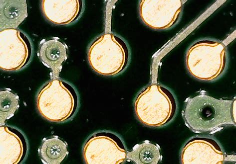
Visual Inspection
Visual inspection is the most basic form of soldermask quality control. This involves examining the PCB under magnification to check for any visible defects, such as voids, pinholes, or inconsistent coverage. Automated Optical Inspection (AOI) systems can be used to quickly scan PCBs for soldermask defects and provide quantitative measurements of soldermask quality.
Adhesion Testing
Soldermask adhesion testing is performed to ensure that the soldermask is securely bonded to the PCB surface. Common adhesion testing methods include:
-
Tape test: A piece of adhesive tape is applied to the soldermask surface and then peeled off. The amount of soldermask removed by the tape provides an indication of its adhesion strength.
-
Cross-hatch test: A pattern of intersecting cuts is made in the soldermask surface, and tape is applied and peeled off. The percentage of soldermask remaining on the PCB after tape removal is used to assess adhesion.
Insulation Resistance Testing
Insulation resistance (IR) testing is used to verify the electrical insulating properties of the soldermask. This test involves applying a high voltage between the copper traces and measuring the resistance of the soldermask. A high IR value indicates good insulating properties and minimal risk of short circuits.
FAQ
-
Q: What is the purpose of soldermask on a PCB?
A: Soldermask serves two main purposes on a PCB: protecting the copper traces from oxidation and other environmental factors, and preventing solder from adhering to areas where it is not intended, thus avoiding solder bridges and short circuits. -
Q: What are the most common colors of soldermask?
A: The most common soldermask color is green, but other popular colors include red, blue, yellow, black, and white. The choice of color is often based on aesthetic preferences, branding requirements, or functional considerations such as improving contrast for easier inspection. -
Q: What is the difference between LPISM and DFISM?
A: LPISM (Liquid Photoimageable Soldermask) is applied to the PCB surface using screen printing, while DFISM (Dry Film Photoimageable Soldermask) is supplied as a photosensitive film that is laminated onto the PCB surface. DFISM generally offers better thickness control and resolution, while LPISM provides better adhesion and lower cost. -
Q: What is soldermask clearance, and why is it important?
A: Soldermask clearance refers to the minimum distance between the edge of a soldermask opening and the edge of a copper pad or trace. Adequate soldermask clearance is necessary to ensure that the soldermask adheres properly to the PCB surface and does not interfere with the soldering process. -
Q: What are some advanced soldermask techniques?
A: Two advanced soldermask techniques are peelable soldermask and direct imaging soldermask. Peelable soldermask is designed to be easily removed after soldering, allowing for rework or additional component assembly. Direct imaging soldermask uses a high-precision laser or LED light source to directly expose the soldermask material, offering higher resolution and faster processing times compared to traditional methods.
Conclusion
Soldermask is an essential component in the production of high-quality, reliable PCBs. By protecting copper traces, preventing solder bridges, and enhancing PCB aesthetics, soldermask plays a vital role in ensuring the proper function and longevity of electronic devices. Understanding the properties, application methods, design considerations, and quality control techniques associated with soldermask is crucial for PCB designers, manufacturers, and end-users alike.
As PCB technology continues to advance, with increasing miniaturization and higher component densities, the importance of soldermask will only grow. Innovations in soldermask materials, application methods, and design tools will be necessary to keep pace with the evolving demands of the electronics industry.
By mastering the fundamentals of soldermask and staying up-to-date with the latest developments in this field, PCB professionals can continue to push the boundaries of what is possible in electronic design and manufacturing.


Leave a Reply