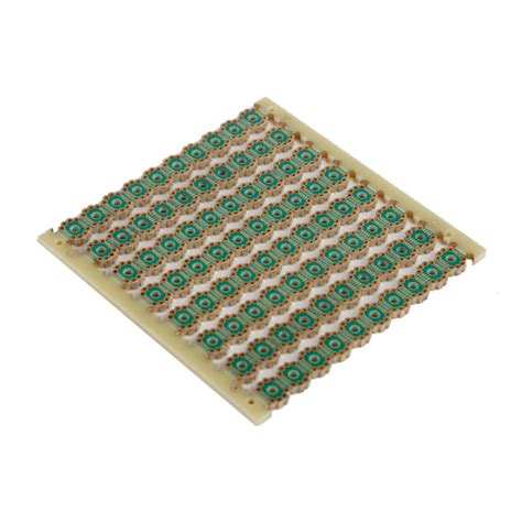
Introduction to Castellated-Hole-PCB
Castellated-Hole-PCB, also known as castellated printed circuit boards or castellated hole technology, is a specialized PCB design that features a series of semi-circular holes or slots along the edges of the board. These holes, resembling the battlements of a castle, serve as electrical contacts and mounting points for connecting multiple PCBs or modules together. This innovative design offers several advantages over traditional PCB interconnection methods, making it an increasingly popular choice for various electronic applications.
Benefits of Castellated-Hole-PCB
- Compact size and space-saving design
- Simplified assembly process
- Enhanced mechanical stability
- Improved electrical performance
- Cost-effective solution for modular electronics
PCB Manufacturing Process Overview
To fully understand the production of Castellated-Hole-PCB, it is essential to have a basic knowledge of the PCB manufacturing process. The typical steps involved in PCB fabrication include:
- PCB Design and Layout
- PCB Material Selection
- PCB Fabrication
- Copper Clad Laminate Preparation
- Drilling and Hole Plating
- Copper Patterning
- Soldermask Application
- Silkscreen Printing
- Surface Finish Application
- PCB Assembly
- PCB Testing and Inspection

Castellated-Hole-PCB Design Considerations
When designing a Castellated-Hole-PCB, several key factors must be taken into account to ensure optimal performance and manufacturability:
Hole Size and Spacing
The size and spacing of the castellated holes are crucial for proper interconnection and mechanical stability. Typical hole diameters range from 0.5mm to 1.0mm, with a minimum spacing of 0.5mm between holes. The exact dimensions may vary depending on the specific application and PCB manufacturing capabilities.
PCB Thickness
The thickness of the PCB material plays a significant role in the strength and durability of the castellated holes. Thinner PCBs may be more susceptible to damage during the milling process, while thicker PCBs may require larger hole diameters to maintain structural integrity. A common PCB thickness for Castellated-Hole-PCB is 1.6mm, although other thicknesses can be used based on design requirements.
Copper Plating Thickness
To ensure reliable electrical connections, the castellated holes must be plated with a sufficient amount of copper. The copper plating thickness typically ranges from 25μm to 35μm, depending on the current carrying capacity and mechanical stress requirements of the application.
Soldermask and Silkscreen
Applying soldermask and silkscreen to the Castellated-Hole-PCB helps protect the copper traces and provides clear labeling for assembly and debugging purposes. The soldermask should be applied carefully to avoid excessive coverage of the castellated holes, which could hinder the soldering process.

Castellated-Hole-PCB Fabrication Techniques
There are two primary methods for fabricating Castellated-Hole-PCBs: routing and milling.
Routing Method
The routing method involves using a CNC router to create the castellated holes along the edges of the PCB. This process is typically performed after the standard PCB fabrication steps, such as copper patterning and soldermask application. The main advantage of the routing method is its ability to produce precise and consistent hole sizes and spacing.
Milling Method
The milling method uses a specialized milling machine to create the castellated holes. This process is performed on individual PCBs after they have been cut from the larger panel. Milling offers greater flexibility in terms of hole size and shape, as well as the ability to create castellated holes on non-rectangular PCB shapes.

Castellated-Hole-PCB Assembly Techniques
Assembling Castellated-Hole-PCBs requires special considerations to ensure proper alignment and reliable electrical connections.
Hand Soldering
For low-volume production or prototype assembly, hand soldering is a viable option. The castellated holes are first filled with solder paste using a syringe or stencil. The PCBs are then aligned and held in place while the solder is reflowed using a soldering iron or hot air gun. Hand soldering allows for greater control and flexibility but is more time-consuming and labor-intensive compared to automated methods.
Reflow Soldering
Reflow soldering is the preferred method for high-volume production of Castellated-Hole-PCBs. In this process, solder paste is applied to the castellated holes using a stencil or solder paste dispenser. The PCBs are then aligned and placed in a reflow oven, where the solder is melted and forms a reliable electrical and mechanical connection between the boards. Reflow soldering offers consistent results and faster assembly times but requires careful control of the solder paste application and reflow temperature profile.
Quality Control and Testing
To ensure the reliability and performance of Castellated-Hole-PCBs, strict quality control measures and thorough testing procedures must be implemented throughout the manufacturing process.
Visual Inspection
Visual inspection is the first line of defense against defects and anomalies in Castellated-Hole-PCBs. Trained operators or automated optical inspection (AOI) systems check for issues such as misaligned holes, incomplete solder fillets, and damaged copper traces.
Electrical Testing
Electrical testing is essential to verify the continuity and isolation of the electrical connections formed by the castellated holes. Common testing methods include flying probe testing, bed-of-nails testing, and in-circuit testing (ICT). These tests help identify short circuits, open circuits, and other electrical faults that could compromise the functionality of the assembled PCBs.
Mechanical Testing
Mechanical testing is performed to assess the strength and durability of the castellated hole connections. Shear strength testing and pull testing are commonly used to evaluate the ability of the solder joints to withstand the stresses encountered during assembly, handling, and operation.
Environmental Testing
Environmental testing is necessary to ensure that Castellated-Hole-PCBs can perform reliably under the expected operating conditions. Tests such as thermal cycling, humidity exposure, and vibration testing help identify potential weaknesses in the design or assembly process that could lead to premature failure in the field.
Applications of Castellated-Hole-PCB
Castellated-Hole-PCBs find applications in a wide range of industries and products where modular design, compact size, and reliable interconnections are essential.
IoT Devices
Internet of Things (IoT) devices often employ Castellated-Hole-PCBs to create compact, modular sensor nodes and communication modules. The castellated hole design allows for easy stacking and interconnection of multiple PCBs, enabling the creation of customized IoT solutions with reduced development time and cost.
Wearable Electronics
Wearable electronics, such as smartwatches and fitness trackers, benefit from the space-saving design and robust connections provided by Castellated-Hole-PCBs. The modular nature of castellated hole technology allows for the integration of various sensors, displays, and communication modules in a compact and lightweight form factor.
Automotive Electronics
Castellated-Hole-PCBs are increasingly used in automotive electronics due to their ability to withstand the harsh environmental conditions and vibrations encountered in vehicles. Applications include advanced driver assistance systems (ADAS), infotainment systems, and powertrain control modules.
Medical Devices
Medical devices, such as implantable sensors and wearable monitoring systems, rely on Castellated-Hole-PCBs for their compact size, reliable interconnections, and ability to withstand sterilization processes. The modular design approach enabled by castellated hole technology allows for the creation of customized medical devices tailored to specific patient needs.
Frequently Asked Questions (FAQ)
1. What is the minimum hole size for Castellated-Hole-PCBs?
The minimum hole size for Castellated-Hole-PCBs typically ranges from 0.5mm to 0.8mm, depending on the PCB manufacturer’s capabilities and the specific design requirements. Smaller hole sizes may be possible but can increase the manufacturing complexity and cost.
2. Can Castellated-Hole-PCBs be used with surface-mount components?
Yes, Castellated-Hole-PCBs are compatible with surface-mount components. The PCB design can incorporate both castellated holes for board-to-board interconnections and traditional SMD pads for component assembly. This hybrid approach allows for greater flexibility in the overall system design.
3. How does the cost of Castellated-Hole-PCBs compare to traditional PCBs?
The cost of Castellated-Hole-PCBs is generally higher than traditional PCBs due to the additional manufacturing steps involved, such as milling or routing the castellated holes. However, the overall system cost can be lower when considering the simplified assembly process, reduced connector costs, and improved reliability offered by castellated hole technology.
4. Are there any limitations on the number of layers in a Castellated-Hole-PCB?
Castellated-Hole-PCBs can be designed with multiple layers, just like traditional PCBs. The number of layers is limited only by the capabilities of the PCB manufacturer and the specific design requirements. However, it is essential to consider the impact of the layer count on the manufacturability and cost of the PCB.
5. Can Castellated-Hole-PCBs be used in high-temperature applications?
Yes, Castellated-Hole-PCBs can be used in high-temperature applications, provided that the appropriate PCB materials and solder alloys are selected. High-temperature laminates, such as polyimide or PTFE, and lead-free solder alloys with higher melting points can ensure reliable performance in elevated temperature environments.
Conclusion
Castellated-Hole-PCB technology offers a unique and advantageous solution for creating modular, compact, and reliable electronic assemblies. By understanding the design considerations, fabrication techniques, assembly methods, and quality control measures involved in the production of Castellated-Hole-PCBs, engineers and manufacturers can leverage this technology to create innovative and high-performance products across a wide range of industries.
As the demand for smaller, more integrated, and more reliable electronic systems continues to grow, Castellated-Hole-PCBs will play an increasingly important role in shaping the future of electronics design and manufacturing.
| Castellated-Hole-PCB vs. Traditional PCB |
|---|
| Feature |
| ———————– |
| Board-to-board |
| interconnection |
| ———————– |
| Assembly complexity |
| ———————– |
| Connector cost |
| ———————– |
| Space utilization |
| ———————– |
| Mechanical stability |
| ———————– |
| Design flexibility |
| ———————– |
| Manufacturing cost |
| ———————– |
| Overall system cost |


Leave a Reply