Introduction to PCB Wiring
Printed Circuit Board (PCB) wiring is a crucial aspect of electronic design and manufacturing. Proper PCB wiring ensures the reliable operation of electronic devices, minimizes signal interference, and enhances the overall performance of the system. In this comprehensive guide, we will explore the essential tips and techniques for effective PCB wiring, helping you create high-quality and robust electronic products.
Understanding the Basics of PCB Wiring
What is PCB Wiring?
PCB wiring refers to the process of connecting various components on a printed circuit board using conductive traces, pads, and vias. These connections allow electrical signals to flow between components, enabling the desired functionality of the electronic device.
Types of PCB Wiring
There are several types of PCB wiring techniques, each with its own advantages and applications:
- Through-hole Wiring: Components are inserted into drilled holes on the PCB and soldered on the opposite side.
- Surface Mount Wiring: Components are mounted directly onto the surface of the PCB using solder pads.
- Mixed Technology Wiring: A combination of through-hole and surface mount wiring techniques.
- Wire Wrapping: A method of connecting components using thin insulated wires wrapped around square posts.
Importance of Proper PCB Wiring
Proper PCB wiring is essential for several reasons:
- Reliability: Well-designed and executed PCB wiring ensures the reliable operation of electronic devices, reducing the risk of failures and malfunctions.
- Signal Integrity: Proper wiring techniques minimize signal interference, crosstalk, and noise, resulting in cleaner and more stable signals.
- Manufacturability: Following best practices in PCB wiring simplifies the manufacturing process, reduces assembly errors, and improves production efficiency.
- Thermal Management: Appropriate wiring techniques help dissipate heat generated by components, preventing overheating and ensuring optimal performance.
PCB Wiring Design Considerations
Component Placement
Proper component placement is crucial for effective PCB wiring. Consider the following guidelines:
- Functional Grouping: Arrange components based on their functional relationships to minimize the length of connections and improve signal integrity.
- Orientation: Orient components in a way that facilitates easy wiring and minimizes the crossing of traces.
- Spacing: Ensure adequate spacing between components to accommodate wiring and prevent interference.
- Thermal Considerations: Place heat-generating components strategically to optimize heat dissipation and prevent thermal issues.
Trace Routing
Trace routing is the process of creating conductive paths between components on the PCB. Consider these factors:
- Width: Choose appropriate trace widths based on the current carrying requirements and manufacturing constraints.
- Spacing: Maintain sufficient spacing between traces to minimize crosstalk and signal interference.
- Length: Minimize trace lengths to reduce signal delays and improve overall performance.
- Angles: Use 45-degree angles or rounded corners for trace routing to minimize signal reflections and improve manufacturability.
Power and Ground Planes
Incorporating power and ground planes in PCB wiring offers several benefits:
- Reduced Impedance: Planes provide low-impedance paths for power and ground, minimizing voltage drops and ensuring stable power distribution.
- Shielding: Planes act as shields, reducing electromagnetic interference (EMI) and improving signal integrity.
- Heat Dissipation: Planes help dissipate heat generated by components, preventing thermal issues.
Vias and Layer Transitions
Vias and layer transitions are essential for connecting traces across different layers of the PCB. Consider the following:
- Via Size: Choose appropriate via sizes based on the current carrying requirements and manufacturing constraints.
- Via Placement: Place vias strategically to minimize signal reflections and improve signal integrity.
- Layer Transitions: Use smooth layer transitions to minimize signal discontinuities and reflections.
- Via Stitching: Implement via stitching techniques to improve power and ground connectivity and reduce EMI.
Signal Integrity and EMI Considerations
Signal integrity and EMI are critical aspects of PCB wiring. Consider these guidelines:
- Impedance Matching: Match the impedance of traces to the source and load impedances to minimize signal reflections and ensure proper signal termination.
- Crosstalk Reduction: Implement techniques such as guard traces, differential pairs, and proper spacing to minimize crosstalk between signals.
- Decoupling and Filtering: Use decoupling capacitors and filtering techniques to suppress noise and stabilize power supply voltages.
- Shielding: Implement shielding techniques, such as grounded traces or shielding cans, to reduce EMI and improve signal integrity.

PCB Wiring Manufacturing Considerations
PCB Fabrication Processes
Understanding the PCB fabrication processes is essential for designing manufacturable PCB wiring. Consider the following:
- Copper Thickness: Choose appropriate copper thicknesses based on the current carrying requirements and manufacturing constraints.
- Trace and Spacing Tolerances: Adhere to the minimum trace width and spacing tolerances specified by the PCB manufacturer to ensure manufacturability.
- Via and Hole Sizes: Follow the manufacturer’s guidelines for minimum via and hole sizes to ensure proper plating and reliability.
- Solder Mask and Silkscreen: Include solder mask and silkscreen layers to protect the PCB and provide clear component markings.
Assembly and Soldering Techniques
Proper assembly and soldering techniques are crucial for reliable PCB wiring. Consider these guidelines:
- Component Handling: Use appropriate handling techniques and equipment to prevent damage to components during assembly.
- Solder Paste Application: Apply solder paste accurately and consistently using stencils or dispensing methods.
- Reflow Soldering: Follow the recommended reflow soldering profile for the specific components and PCB materials.
- Wave Soldering: Use wave soldering techniques for through-hole components, ensuring proper preheat and solder flow.
Inspection and Testing
Inspection and testing are essential for ensuring the quality and reliability of PCB wiring. Consider the following:
- Visual Inspection: Perform visual inspections to identify any visible defects, such as bridging, insufficient solder, or component misalignment.
- Automated Optical Inspection (AOI): Use AOI systems to detect assembly defects and ensure consistent quality.
- In-Circuit Testing (ICT): Perform in-circuit testing to verify the presence and correct functioning of components.
- Functional Testing: Conduct functional tests to validate the overall performance and functionality of the assembled PCB.
Best Practices for PCB Wiring
Documentation and Version Control
Proper documentation and version control are essential for effective PCB wiring. Consider these practices:
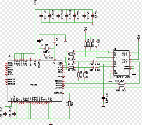
- Schematic Diagrams: Create clear and accurate schematic diagrams that represent the electrical connections and component information.
- PCB Layout Files: Maintain well-organized and properly named PCB layout files for easy reference and modification.
- Bill of Materials (BOM): Generate a comprehensive BOM that lists all the components, quantities, and specifications required for the PCB assembly.
- Version Control: Implement version control systems to track changes, collaborate with team members, and maintain a history of revisions.
Collaboration and Communication
Effective collaboration and communication among team members are crucial for successful PCB wiring projects. Consider the following:
- Design Reviews: Conduct regular design reviews to gather feedback, identify potential issues, and ensure adherence to design guidelines.
- Documentation Sharing: Use collaborative tools and platforms to share and access design documentation, such as schematics, layouts, and BOMs.
- Communication Channels: Establish clear communication channels, such as email, instant messaging, or project management tools, to facilitate effective communication among team members.
- Stakeholder Involvement: Engage stakeholders, such as manufacturers, assemblers, and end-users, to gather their input and ensure alignment with their requirements.
Continuous Improvement and Learning
Continuous improvement and learning are essential for staying up-to-date with the latest PCB wiring techniques and technologies. Consider these practices:
- Training and Workshops: Participate in training sessions and workshops to enhance your knowledge and skills in PCB wiring design and manufacturing.
- Industry Standards: Stay informed about industry standards and guidelines related to PCB wiring, such as IPC standards, to ensure compliance and best practices.
- Peer Review and Feedback: Seek peer review and feedback on your PCB wiring designs to identify areas for improvement and learn from the experiences of others.
- Continuous Optimization: Regularly review and optimize your PCB wiring processes to improve efficiency, reliability, and cost-effectiveness.
Frequently Asked Questions (FAQ)
-
Q: What are the most common mistakes to avoid in PCB wiring?
A: Some common mistakes to avoid in PCB wiring include incorrect component placement, insufficient trace widths, improper spacing between traces, neglecting signal integrity considerations, and failing to adhere to manufacturing constraints. -
Q: How can I ensure the manufacturability of my PCB wiring design?
A: To ensure the manufacturability of your PCB wiring design, follow the guidelines provided by your PCB manufacturer, adhere to industry standards, use appropriate trace widths and spacings, incorporate design for manufacturing (DFM) principles, and conduct thorough design reviews and simulations. -
Q: What are the key considerations for high-speed PCB wiring?
A: Key considerations for high-speed PCB wiring include impedance matching, minimizing signal reflections, reducing crosstalk, implementing proper termination techniques, using controlled impedance traces, and paying attention to signal integrity and EMI mitigation strategies. -
Q: How can I minimize signal interference in PCB wiring?
A: To minimize signal interference in PCB wiring, use proper grounding techniques, implement power and ground planes, route signals away from noise sources, use differential signaling for sensitive signals, and incorporate filtering and decoupling techniques. -
Q: What are the benefits of using PCB design software for wiring?
A: PCB design software offers several benefits for wiring, including automated routing, design rule checks (DRC), simulation capabilities, component libraries, collaboration features, and the ability to generate manufacturing files and documentation efficiently.
Conclusion
PCB wiring is a critical aspect of electronic design and manufacturing that requires careful consideration and adherence to best practices. By understanding the fundamentals of PCB wiring, applying design considerations, and following manufacturing guidelines, you can create high-quality and reliable electronic products.
Remember to prioritize component placement, trace routing, power and ground planes, signal integrity, and EMI mitigation techniques. Collaborate effectively with team members, maintain proper documentation, and continuously improve your PCB wiring skills and knowledge.
By implementing the tips and essentials covered in this comprehensive guide, you can ensure the success of your PCB wiring projects and deliver robust and high-performing electronic devices.
Leave a Reply