What is a PCB Stencil?
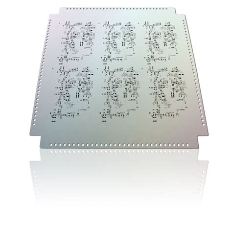
A PCB stencil, also known as a solder paste stencil, is a thin sheet of material, typically stainless steel or polyimide, that is used to apply solder paste onto a printed circuit board (PCB) during the surface mount technology (SMT) assembly process. The stencil has apertures or openings that correspond to the pads on the PCB where components will be placed. When solder paste is applied over the stencil, it is deposited through these openings onto the pads in a precise and controlled manner.
PCB stencils play a crucial role in ensuring the quality and reliability of the soldering process. They help to achieve the correct amount and placement of solder paste on the pads, which is essential for creating strong and reliable solder joints between the components and the PCB.
Types of PCB Stencils
There are several types of PCB stencils available, each with its own characteristics and advantages. The choice of stencil type depends on various factors such as the complexity of the PCB design, the size and pitch of the components, the production volume, and the budget. Here are the main types of PCB stencils:
1. Stainless Steel Stencils
Stainless steel stencils are the most common type of PCB stencils used in the industry. They are made from high-quality stainless steel, typically with a thickness ranging from 0.1 mm to 0.2 mm (4 to 8 mils). Stainless steel stencils are known for their durability, precision, and long lifespan.
Advantages of Stainless Steel Stencils:
- High precision and accuracy
- Excellent durability and long lifespan
- Suitable for high-volume production
- Compatible with a wide range of solder paste types
- Easy to clean and maintain
Disadvantages of Stainless Steel Stencils:
- Higher initial cost compared to other stencil types
- Requires careful handling to prevent damage
- May require additional support for very fine pitch components
2. Polyimide Stencils
Polyimide stencils, also known as polymer stencils or plastic stencils, are made from a flexible and durable polymer material. They are commonly used for low-volume production runs, prototypes, and rework applications. Polyimide stencils are typically thinner than stainless steel stencils, with a thickness ranging from 0.05 mm to 0.13 mm (2 to 5 mils).
Advantages of Polyimide Stencils:
- Lower cost compared to stainless steel stencils
- Flexibility allows for conformity to uneven surfaces
- Suitable for low-volume production and prototyping
- Ideal for rework and repair applications
- Easier to store and transport
Disadvantages of Polyimide Stencils:
- Lower durability compared to stainless steel stencils
- Not suitable for high-volume production
- Limited compatibility with certain solder paste types
- May require more frequent cleaning and maintenance
3. Electroformed Nickel Stencils
Electroformed nickel stencils are created using an electroplating process, where nickel is deposited onto a photoresist-patterned substrate. This process allows for the creation of highly precise and intricate stencil designs with very fine apertures. Electroformed nickel stencils are typically used for applications that require extremely fine pitch components or high-density PCB layouts.
Advantages of Electroformed Nickel Stencils:
- Extremely high precision and accuracy
- Capable of producing very fine apertures (down to 0.05 mm or 2 mils)
- Smooth aperture walls for improved paste release
- Suitable for high-density PCB layouts and fine pitch components
Disadvantages of Electroformed Nickel Stencils:
- Higher cost compared to other stencil types
- Longer lead time for production
- Limited thickness options (typically 0.05 mm to 0.1 mm or 2 to 4 mils)
- Requires careful handling and storage to prevent damage
4. Laser-Cut Stencils
Laser-cut stencils are manufactured using high-precision laser cutting technology. This process allows for the creation of complex stencil designs with intricate aperture shapes and sizes. Laser-cut stencils can be made from various materials, including stainless steel, polyimide, and nickel.
Advantages of Laser-Cut Stencils:
- High precision and accuracy
- Capability to create complex aperture shapes and sizes
- Fast production times
- Suitable for prototyping and low-volume production
- Compatible with a wide range of materials
Disadvantages of Laser-Cut Stencils:
- Higher cost compared to traditional stencil manufacturing methods
- May have slightly rougher aperture walls compared to other stencil types
- Limited thickness options depending on the material used
5. Hybrid Stencils
Hybrid stencils combine multiple stencil technologies to achieve the benefits of each type. For example, a hybrid stencil may consist of a stainless steel frame with a polyimide or electroformed nickel foil attached to it. This combination allows for the durability and stability of the stainless steel frame while leveraging the precision and flexibility of the polyimide or nickel foil.
Advantages of Hybrid Stencils:
- Combines the benefits of multiple stencil technologies
- Offers a balance between durability and precision
- Suitable for applications with varying component sizes and pitches
- Provides flexibility in design and manufacturing
Disadvantages of Hybrid Stencils:
- Higher cost compared to single-material stencils
- May require specialized manufacturing processes
- Potential for compatibility issues between different materials

Choosing the Right PCB Stencil
When selecting a PCB stencil for your assembly process, consider the following factors:
-
PCB Design Complexity: Evaluate the complexity of your PCB design, including the component sizes, pitches, and layout density. More complex designs may require higher precision stencils like electroformed nickel or laser-cut stencils.
-
Production Volume: Consider the production volume of your PCB Assembly. For high-volume production, durable stencils like stainless steel are preferred. For low-volume runs or prototyping, polyimide or laser-cut stencils may be more cost-effective.
-
Solder Paste Compatibility: Ensure that the stencil material is compatible with the solder paste you intend to use. Some solder paste formulations may have specific requirements for stencil materials to achieve optimal performance.
-
Budget: Compare the costs of different stencil types and consider your budget constraints. While higher-precision stencils may have a higher initial cost, they can provide long-term benefits in terms of quality and reliability.
-
Maintenance and Cleaning: Consider the ease of maintenance and cleaning for the chosen stencil type. Stainless steel stencils are generally easier to clean and maintain compared to polyimide or electroformed nickel stencils.
-
Supplier Capabilities: Evaluate the capabilities of your PCB stencil supplier, including their manufacturing processes, quality control measures, and lead times. Choose a supplier that can consistently deliver high-quality stencils that meet your specifications.

PCB Stencil Design Considerations
To ensure the optimal performance of your PCB stencil, consider the following design guidelines:
-
Aperture Size and Shape: The size and shape of the stencil apertures should be carefully designed to ensure the proper amount of solder paste is deposited on the pads. Consider factors such as the component size, pitch, and pad geometry when determining the aperture dimensions.
-
Stencil Thickness: The thickness of the stencil plays a crucial role in controlling the amount of solder paste deposited. Thicker stencils (0.15 mm to 0.2 mm or 6 to 8 mils) are typically used for larger components or higher-volume solder paste deposits. Thinner stencils (0.1 mm to 0.15 mm or 4 to 6 mils) are suitable for smaller components or finer pitch applications.
-
Aperture Wall Geometry: The geometry of the aperture walls can affect the release of solder paste during the printing process. Tapered aperture walls or rounded corners can improve paste release and reduce the risk of clogging.
-
Fiducial Marks: Include fiducial marks on the stencil to ensure proper alignment with the PCB during the solder paste printing process. Fiducial marks should be strategically placed and sized for accurate recognition by the solder paste inspection system.
-
Stencil Frame: Consider the size and material of the stencil frame to ensure compatibility with your solder paste printer and to provide adequate support for the stencil foil.
-
Overprinting and Understencil Cleaning: Plan for overprinting and understencil cleaning in your stencil design. Provide sufficient space around the apertures to accommodate solder paste overflow and to facilitate effective cleaning of the stencil underside.

PCB Stencil Maintenance and Cleaning
Proper maintenance and cleaning of your PCB stencil are essential for ensuring consistent solder paste printing quality and extending the stencil’s lifespan. Follow these guidelines for stencil maintenance and cleaning:
-
Regular Inspection: Regularly inspect the stencil for signs of wear, damage, or clogging. Check for bent or damaged apertures, solder paste buildup, or any other irregularities that may affect the printing process.
-
Understencil Cleaning: Perform understencil cleaning at regular intervals during the printing process to prevent solder paste accumulation and clogging. Use appropriate cleaning materials and techniques, such as specialized understencil wiping rolls or solvents, to remove excess solder paste effectively.
-
Stencil Storage: Store the stencil properly when not in use to prevent damage or contamination. Use a stencil storage rack or container that keeps the stencil flat and protected from dust, moisture, and other environmental factors.
-
Handling and Transportation: Handle the stencil with care during installation, removal, and transportation to avoid bending, warping, or other physical damage. Use proper handling techniques and protective packaging when transporting the stencil between locations.
-
Periodic Deep Cleaning: Perform a thorough deep cleaning of the stencil at regular intervals, depending on the usage and solder paste type. Use specialized stencil cleaning solutions and equipment, such as ultrasonic cleaners or stencil washing machines, to remove stubborn solder paste residues and ensure a clean and debris-free stencil surface.
By following these maintenance and cleaning practices, you can extend the life of your PCB stencil, minimize printing defects, and ensure consistent solder paste deposition quality throughout your PCB assembly process.
Frequently Asked Questions (FAQ)
- What is the difference between a solder paste stencil and a solder mask?
- A solder paste stencil is used to apply solder paste onto the PCB pads during the solder paste printing process. It is a separate component that is placed on top of the PCB.
-
A solder mask, on the other hand, is a permanent protective layer applied directly onto the PCB surface. It serves to insulate and protect the copper traces while exposing only the pads where components will be soldered.
-
Can I reuse a PCB stencil?
- Yes, PCB stencils can be reused multiple times with proper cleaning and maintenance. Stainless steel stencils, in particular, are known for their durability and long lifespan.
-
However, the number of reuses depends on factors such as the stencil material, solder paste type, and the frequency and effectiveness of cleaning and maintenance procedures.
-
How often should I clean my PCB stencil?
- The frequency of cleaning depends on the solder paste type, printing volume, and environmental conditions. As a general guideline, perform understencil cleaning at regular intervals during the printing process, such as every 1-2 hours or after a specific number of prints.
-
Additionally, perform a thorough deep cleaning of the stencil at least once per shift or as recommended by the solder paste manufacturer.
-
How do I store my PCB stencil when not in use?
- Store the stencil in a clean, dry, and dust-free environment. Use a stencil storage rack or container that keeps the stencil flat and protected from damage or contamination.
-
Avoid storing the stencil in areas with high humidity or temperature fluctuations, as these conditions can lead to stencil warping or corrosion.
-
Can I modify an existing PCB stencil for a new design?
- In most cases, modifying an existing stencil for a new PCB design is not recommended, as it may compromise the stencil’s integrity and lead to printing defects.
- It is generally more cost-effective and reliable to fabricate a new stencil specifically designed for the new PCB layout, ensuring optimal aperture sizes, shapes, and placement.
By understanding the different types of PCB stencils, their characteristics, and the design and maintenance considerations, you can select the most suitable stencil for your PCB assembly process. A well-designed and properly maintained PCB stencil is crucial for achieving high-quality solder paste deposition, reliable solder joints, and overall PCB assembly success.


Leave a Reply