What is a PCB Stencil?
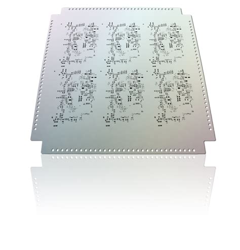
A printed circuit board (PCB) stencil, also known as a solder paste stencil, is a thin sheet of stainless steel or polyester with laser-cut openings that correspond to the pads on a PCB. The stencil is used to apply solder paste onto the PCB pads with high precision before placing components during the assembly process. PCB stencils ensure consistent and accurate solder paste application, which is crucial for achieving reliable solder joints and preventing defects.
Types of PCB Stencils
There are two main types of PCB stencils:
-
Stainless Steel Stencils: These stencils are made from high-quality stainless steel and offer excellent durability, stability, and precision. They are suitable for high-volume production and fine-pitch components.
-
Polyester Stencils: Also known as mesh stencils, these are made from a fine polyester mesh coated with a photosensitive emulsion. Polyester stencils are less expensive and more flexible than stainless steel stencils but have lower durability and precision.
The PCB Screen Printing Stencil Making Process
The process of creating a PCB stencil involves several steps, from design to fabrication. Here’s a detailed overview of the PCB screen printing stencil making process:
Step 1: Stencil Design
The first step in creating a PCB stencil is to design the stencil based on the PCB layout. The stencil design should include the following considerations:
- Aperture Size: The size of the openings in the stencil, which determines the amount of solder paste deposited on the pads.
- Aperture Shape: The shape of the openings, which can be rectangular, circular, or custom-shaped to accommodate different pad geometries.
- Stencil Thickness: The thickness of the stencil, which affects the volume of solder paste deposited and the printing process.
| Stencil Thickness | Typical Application |
|---|---|
| 100-150 μm | Standard SMT components |
| 150-200 μm | Large SMT components, connectors |
| 200-250 μm | Power components, through-hole components |
Step 2: Stencil Fabrication
Once the stencil design is finalized, the stencil is fabricated using one of the following methods:
Chemical Etching
Chemical etching is a subtractive process that involves the following steps:
- A photosensitive resist is applied to both sides of a stainless steel sheet.
- The stencil design is exposed onto the resist using UV light.
- The unexposed resist is removed, leaving the stencil pattern on the metal surface.
- The metal is etched using a chemical solution, creating the openings in the stencil.
- The remaining resist is removed, and the stencil is cleaned and inspected.
Laser Cutting
Laser cutting is a precise and fast method for fabricating PCB stencils. The process involves the following steps:
- A high-power laser beam is focused onto the stainless steel sheet.
- The laser beam cuts the stencil pattern by vaporizing the metal along the cut path.
- The stencil is cleaned and inspected for any defects or irregularities.
Laser-cut stencils offer higher precision and faster turnaround times compared to chemically etched stencils.
Step 3: Stencil Inspection
After fabrication, the PCB stencil undergoes a thorough inspection to ensure its quality and conformance to the design specifications. The inspection process may include:
- Visual inspection for any visible defects, such as incomplete apertures or surface damage.
- Dimensional verification using optical or mechanical measuring tools to check aperture sizes and positions.
- Thickness measurement to ensure uniform thickness across the stencil.
Stencils that pass the inspection are ready for use in the PCB assembly process.
Step 4: Stencil Maintenance and Storage
Proper maintenance and storage of PCB stencils are essential for ensuring their longevity and consistent performance. Some best practices include:
- Cleaning: Regular cleaning of the stencil using isopropyl alcohol or a specialized stencil cleaner to remove solder paste residue and prevent clogging of apertures.
- Handling: Using gloves when handling stencils to avoid contamination and minimize the risk of damage.
- Storage: Storing stencils in a clean, dry environment, preferably in a vertical position to prevent warping or damage.
| Stencil Material | Cleaning Method | Storage Conditions |
|---|---|---|
| Stainless Steel | Isopropyl alcohol, ultrasonic cleaning | Vertical storage, room temperature |
| Polyester | Mild detergent, manual cleaning | Flat storage, room temperature, low humidity |

Advantages of Using PCB Stencils
Using PCB stencils in the assembly process offers several advantages, including:
- Consistency: Stencils ensure consistent solder paste deposition across the PCB, minimizing variations in solder joint quality.
- Precision: Laser-cut stencils provide high precision in solder paste application, enabling the assembly of fine-pitch components and high-density PCBs.
- Efficiency: Stencil printing is a fast and efficient method for applying solder paste, reducing the time and labor required for manual application.
- Cost-effectiveness: Using stencils reduces solder paste waste and minimizes rework, resulting in lower overall assembly costs.

Challenges and Considerations
While PCB stencils offer many benefits, there are some challenges and considerations to keep in mind:
- Design Complexity: As PCBs become more complex with smaller components and tighter tolerances, stencil design becomes more challenging. Ensuring proper aperture sizes and shapes requires careful consideration of solder paste rheology and component requirements.
- Stencil Thickness: Selecting the appropriate stencil thickness is crucial for achieving the desired solder paste volume and preventing defects such as bridging or insufficient solder joints.
- Stencil Durability: Stencils, especially those made from polyester, have a limited lifespan and may need to be replaced periodically to maintain print quality.
- Printing Parameters: Achieving optimal results with stencil printing requires careful control of printing parameters, such as squeegee pressure, speed, and separation distance.

FAQ
1. What is the difference between a stainless steel and polyester stencil?
Stainless steel stencils are more durable, stable, and precise compared to polyester stencils. They are suitable for high-volume production and fine-pitch components. Polyester stencils, on the other hand, are less expensive and more flexible but have lower durability and precision.
2. How often should I clean my PCB stencil?
PCB stencils should be cleaned regularly to remove solder paste residue and prevent clogging of apertures. The cleaning frequency depends on the production volume and the type of solder paste used. As a general guideline, stencils should be cleaned after every shift or every 1000 prints.
3. Can I reuse a PCB stencil for different PCB designs?
While it is possible to reuse a PCB stencil for different PCB designs, it is not recommended. Each stencil is designed specifically for a particular PCB layout, and using it for a different design may result in incorrect solder paste deposition and assembly defects.
4. How do I select the appropriate stencil thickness for my PCB?
The choice of stencil thickness depends on several factors, including the component sizes, pad dimensions, and solder paste properties. As a general rule, thicker stencils (200-250 μm) are used for larger components and higher solder paste volumes, while thinner stencils (100-150 μm) are used for smaller components and finer pitches. It is essential to consult with your stencil manufacturer or assembly service provider to determine the optimal stencil thickness for your specific PCB design.
5. What are some common defects associated with PCB stencil printing?
Some common defects that can occur during PCB stencil printing include:
- Solder Bridging: Excess solder paste deposition leading to shorts between adjacent pads.
- Insufficient Solder: Insufficient solder paste deposition resulting in weak or open solder joints.
- Solder Balls: Small spheres of solder paste that can cause short circuits or contamination.
- Misalignment: Misalignment between the stencil and the PCB, resulting in off-center solder paste deposition.
These defects can be minimized by using high-quality stencils, maintaining proper printing parameters, and regularly inspecting and cleaning the stencils.
Conclusion
PCB screen printing stencils play a critical role in the PCB assembly process, ensuring consistent and precise solder paste deposition. The stencil-making process involves design, fabrication, inspection, and maintenance steps, each of which contributes to the overall quality and performance of the stencil. By understanding the advantages, challenges, and best practices associated with PCB stencils, manufacturers can optimize their assembly processes and produce high-quality, reliable PCBs.
As PCB designs continue to evolve with smaller components and higher densities, the importance of accurate and efficient solder paste application will only increase. Investing in high-quality PCB stencils and following proper stencil-making processes will help manufacturers stay competitive and meet the growing demands of the electronics industry.


Leave a Reply