What Are PCB Stencils?
PCB stencils, also known as solder paste stencils, are thin metal sheets with cut-outs that match the solder pad pattern on a printed circuit board (PCB). They are used to apply solder paste onto the PCB pads before placing components during the surface mount assembly process. The stencil ensures precise and consistent solder paste application, which is crucial for achieving reliable solder joints and preventing defects.
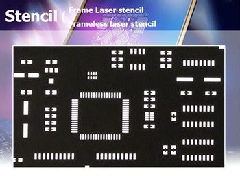
Types of PCB Stencils
There are two main types of PCB stencils:
-
Framed Stencils: These stencils have a metal frame surrounding the stencil area, providing rigidity and ease of handling. They are commonly used in manual assembly processes or with smaller PCBs.
-
Frameless Stencils: These stencils do not have a metal frame and are typically used in automated assembly lines. They are more flexible and can be used with larger PCBs or multiple boards in a panel.
PCB Stencil Materials
PCB stencils are typically made from one of the following materials:
-
Stainless Steel: This is the most common material for PCB stencils due to its durability, stability, and resistance to wear and tear. Stainless steel stencils can be easily cleaned and reused multiple times.
-
Nickel: Nickel stencils are less common but offer similar properties to stainless steel. They are slightly more expensive but can be a good choice for applications requiring high corrosion resistance.
-
Polyimide: Polyimide stencils, also known as kapton stencils, are made from a flexible polymer material. They are used for special applications, such as applying solder paste on flexible circuits or conforming to curved surfaces.
Why Use PCB Stencils?
Using PCB stencils offers several advantages in the PCB Assembly process:
-
Consistency: Stencils ensure a consistent amount of solder paste is applied to each pad, reducing the risk of insufficient or excessive solder joints.
-
Precision: The cut-outs in the stencil match the exact size and shape of the solder pads, allowing for precise solder paste placement.
-
Efficiency: Stencils enable faster solder paste application compared to manual methods, increasing the overall production speed.
-
Cost-effective: Using stencils reduces solder paste waste and minimizes the need for rework, leading to cost savings in the long run.

How To Design PCB Stencils
Designing PCB stencils involves the following steps:
-
Create the PCB layout: Start by designing the PCB layout using electronic design automation (EDA) software. Ensure that the solder pad sizes and shapes are suitable for stencil printing.
-
Generate the stencil data: Most EDA software can generate stencil data directly from the PCB layout. The stencil data includes the aperture sizes, shapes, and locations corresponding to the solder pads.
-
Determine the stencil thickness: The stencil thickness depends on the solder paste volume required for the specific components and the PCB design. A common stencil thickness is 0.1 mm (4 mil) for standard surface mount components.
-
Choose the stencil material: Select the appropriate stencil material based on the application requirements, such as durability, cost, and compatibility with the solder paste.
-
Review and finalize the design: Carefully review the stencil design to ensure all apertures are correctly sized and positioned. Make any necessary adjustments before sending the design for fabrication.

PCB Stencil Fabrication Methods
There are several methods for fabricating PCB stencils, each with its own advantages and limitations:
Laser Cutting
Laser cutting is the most common method for fabricating PCB stencils. It uses a high-powered laser to cut the stencil apertures precisely. Laser cutting offers several benefits:
- High precision and accuracy
- Fast turnaround times
- Suitable for complex designs and fine pitch components
- Minimal wear on the stencil material
However, Laser-Cut Stencils may have slightly rougher aperture edges compared to other methods.
Chemical Etching
Chemical etching involves using a chemical solution to dissolve the unwanted areas of the stencil material, leaving the desired aperture pattern. This method is less common but offers some advantages:
- Smooth aperture edges
- Suitable for large apertures or simple designs
- Lower cost compared to laser cutting
However, chemical etching has limitations in terms of minimum aperture size and may have longer lead times.
Electroforming
Electroforming is a specialized process that involves depositing metal (usually nickel) onto a master pattern to create the stencil. This method is used for high-precision applications and offers unique benefits:
- Extremely smooth aperture walls
- Uniform stencil thickness
- Suitable for ultra-fine pitch components
However, electroformed stencils are more expensive and have longer lead times compared to other methods.

PCB Stencil Design Considerations
When designing PCB stencils, consider the following factors to ensure optimal solder paste deposition and assembly results:
Aperture Size and Shape
The aperture size and shape should match the solder pad dimensions on the PCB. However, some adjustments may be necessary:
-
Aperture Reduction: Slightly reducing the aperture size compared to the pad size (typically by 5-10%) can help prevent solder paste bridging and improve the paste release from the stencil.
-
Aperture Shape: For fine pitch components or small pads, using rounded aperture corners can improve paste release and prevent clogging.
Stencil Thickness
The stencil thickness determines the volume of solder paste deposited on the pads. Consider the following guidelines:
-
For standard surface mount components (SMDs), use a stencil thickness of 0.1 mm (4 mil) to 0.15 mm (6 mil).
-
For larger components or higher solder volume requirements, use a thicker stencil, such as 0.2 mm (8 mil) or more.
-
For fine pitch components or smaller pads, use a thinner stencil, such as 0.08 mm (3 mil) or less, to prevent solder paste bridging.
Aperture Walls
The aperture walls should be smooth and tapered to facilitate solder paste release. Consider the following:
-
Wall Angle: A wall angle of 5-7 degrees is recommended for optimal paste release.
-
Aperture Coining: Coining or stepping the aperture walls can further improve paste release, especially for fine pitch components.
Fiducial Marks
Include fiducial marks on the stencil to aid in alignment with the PCB during the assembly process. Fiducial marks should be located in the corners or edges of the stencil and match the corresponding marks on the PCB.
PCB Stencil Maintenance and Cleaning
Proper maintenance and cleaning of PCB stencils are crucial for ensuring consistent solder paste deposition and preventing defects. Follow these guidelines:
-
Clean the stencil after each use: Use a designated stencil cleaner or isopropyl alcohol to remove any residual solder paste from the apertures and stencil surface.
-
Inspect the stencil regularly: Check for any damage, wear, or clogging of the apertures. Replace the stencil if necessary.
-
Store the stencil properly: Keep the stencil in a protective case or cover when not in use to prevent damage and contamination.
-
Handle the stencil with care: Use gloves when handling the stencil to avoid contamination and prevent skin oils from affecting the solder paste adhesion.
Troubleshooting PCB Stencil Issues
If you encounter problems with solder paste deposition or assembly quality, consider the following troubleshooting tips:
-
Insufficient solder paste: Check if the stencil apertures are clogged or if the stencil is damaged. Ensure the solder paste is at the correct temperature and has not expired.
-
Excessive solder paste: Verify that the stencil thickness and aperture sizes are appropriate for the components. Ensure the stencil is properly aligned with the PCB.
-
Solder paste bridging: Check if the aperture size is too large or if the stencil is too thick. Ensure proper cleaning of the stencil between uses.
-
Poor solder paste release: Verify that the aperture walls are smooth and tapered. Check if the stencil is properly cleaned and not damaged.
FAQ
- What is the typical thickness of a PCB stencil?
-
The typical thickness of a PCB stencil ranges from 0.08 mm (3 mil) to 0.2 mm (8 mil), depending on the component sizes and solder volume requirements.
-
Can PCB stencils be reused?
-
Yes, PCB stencils can be reused multiple times with proper cleaning and maintenance. Stainless steel stencils are particularly durable and suitable for reuse.
-
How often should I clean my PCB stencil?
-
Clean your PCB stencil after each use to remove any residual solder paste and prevent clogging of the apertures. Regular cleaning helps maintain the stencil’s performance and longevity.
-
What is the minimum aperture size for a PCB stencil?
-
The minimum aperture size depends on the fabrication method. Laser-cut stencils can typically achieve aperture sizes as small as 0.1 mm (4 mil), while chemically etched stencils have a larger minimum size.
-
Can I use a PCB stencil for hand soldering?
- While PCB stencils are primarily used for solder paste application in surface mount assembly, they can also be used for hand soldering. Applying solder paste through a stencil can help ensure consistent solder volume and placement, even when hand soldering.
Conclusion
PCB stencils are essential tools in the surface mount assembly process, ensuring precise and consistent solder paste application. By understanding the types, materials, and fabrication methods of PCB stencils, you can make informed decisions when designing and manufacturing your PCBs.
Proper stencil design, considering factors such as aperture size, shape, and thickness, is crucial for achieving optimal solder paste deposition and assembly quality. Regular maintenance, cleaning, and troubleshooting can help extend the life of your stencils and prevent common issues.
By following the guidelines and best practices outlined in this comprehensive guide, you can effectively utilize PCB stencils to streamline your assembly process, reduce defects, and improve the overall quality of your PCBs.


Leave a Reply