What is a PCB?
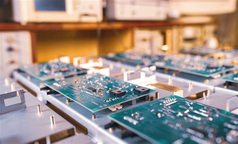
A Printed Circuit Board (PCB) is a thin board made of fiberglass or other composite material, with conductive pathways etched or printed onto the surface. PCBs are used to mechanically support and electrically connect electronic components using conductive traces, pads, and other features. They are the foundation of almost all modern electronic devices, from smartphones and laptops to medical equipment and aerospace systems.
PCBs offer several advantages over other wiring methods, such as wire wrapping or point-to-point construction:
- Compact size
- Reduced wiring errors
- Improved reliability
- Easier mass production
- Lower manufacturing costs
Types of PCBs
There are several types of PCBs, each with its own characteristics and applications:
| PCB Type | Layers | Typical Applications |
|---|---|---|
| Single-layer | 1 | Simple circuits, low-cost devices |
| Double-layer | 2 | Most common, used in a wide range of devices |
| Multi-layer | 4, 6, 8, or more | Complex circuits, high-density devices |
| Flexible | Varies | Wearable electronics, confined spaces |
| Rigid-Flex | Varies | Combines rigid and flexible sections |
The PCB Manufacturing Process
The PCB manufacturing process involves several steps, from design to final inspection. Here’s an overview of the process:
1. PCB Design
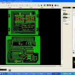
The first step in PCB manufacturing is the design phase. This involves creating a schematic diagram of the circuit, followed by a PCB layout using specialized software. The layout determines the size, shape, and placement of components, as well as the routing of conductive traces.
2. Printing the PCB Artwork
Once the design is finalized, the PCB artwork is printed onto a clear film or directly onto the copper-clad board using a plotter or laser printer. This artwork serves as a template for the subsequent etching process.
3. Etching the Copper
The printed PCB artwork is used to selectively remove unwanted copper from the board. This is typically done using a photoresist and chemical etching process:
- The copper-clad board is coated with a light-sensitive photoresist.
- The PCB artwork is placed on the board and exposed to UV light.
- The exposed photoresist hardens, while the unexposed areas remain soluble.
- The board is placed in a developer solution, which removes the soluble photoresist.
- The board is then placed in an etching solution, which removes the exposed copper.
- Finally, the remaining photoresist is stripped away, leaving only the desired copper traces.
4. Drilling Holes
After etching, holes are drilled into the PCB to accommodate through-hole components and provide interconnections between layers. This is done using computer-controlled drill machines with high precision.
5. Plating and Coating
To improve conductivity and protect the copper traces from oxidation, the PCB undergoes a plating process. This typically involves electroplating a thin layer of copper, followed by a layer of tin-lead alloy (solder).
For multi-layer PCBs, additional insulating layers and copper traces are added, with plated through-holes providing interconnections between layers.
Finally, a protective solder mask is applied to the board, exposing only the areas where components will be soldered.
6. Silkscreen Printing
A silkscreen layer is printed onto the PCB to add text, logos, and component identifiers. This helps with assembly and troubleshooting.
7. Surface Finish
A surface finish is applied to the exposed copper areas to prevent oxidation and improve solderability. Common surface finishes include:
- HASL (Hot Air Solder Leveling)
- ENIG (Electroless Nickel Immersion Gold)
- OSP (Organic Solderability Preservative)
8. Component Assembly
Components are then mounted onto the PCB, either through manual placement or automated pick-and-place machines. Surface-mount components are soldered directly onto pads on the board, while through-hole components are inserted into drilled holes and soldered.
9. Soldering
The assembled PCB is then sent through a reflow oven or wave soldering machine to permanently attach the components to the board. Reflow soldering is used for surface-mount components, while wave soldering is used for through-hole components.
10. Inspection and Testing
After soldering, the PCB undergoes a visual inspection to check for defects such as bridged pins, solder splashes, or misaligned components. Automated optical inspection (AOI) systems are often used for this purpose.
Functional testing is then performed to ensure that the PCB operates as intended. This can involve in-circuit testing (ICT), flying probe testing, or boundary scan testing, depending on the complexity of the board.
11. Finishing and Packaging
Finally, the PCB is cut to its final shape (if part of a panel), cleaned, and coated with a protective finish if required. It is then packaged and shipped to the customer.

Quality Control in PCB Manufacturing
Quality control is crucial throughout the PCB manufacturing process to ensure reliable and consistent performance. Some key quality control measures include:
- Incoming material inspection
- Controlled manufacturing environment (temperature, humidity, cleanliness)
- In-process inspections and testing
- Final inspection and testing
- Traceability and documentation
Challenges in PCB Manufacturing
PCB manufacturing can be complex and challenging, particularly as electronics become more advanced and miniaturized. Some common challenges include:
- Managing high-density designs with fine pitch components
- Maintaining signal integrity in high-speed circuits
- Ensuring proper thermal management
- Dealing with obsolescence and component availability
- Meeting strict quality and reliability requirements
Future Trends in PCB Manufacturing
As technology continues to evolve, PCB manufacturing must adapt to keep pace. Some emerging trends in PCB manufacturing include:
- Increased use of advanced materials (e.g., high-frequency laminates)
- Adoption of embedded components and 3D PCB structures
- Growth of flexible and stretchable electronics
- Integration of sensors and active components into PCBs
- Emphasis on sustainability and eco-friendly manufacturing processes
FAQ
1. What is the difference between a PCB and a PCBA?
A PCB (Printed Circuit Board) is the bare board with etched copper traces, while a PCBA (Printed Circuit Board Assembly) is a PCB with components mounted and soldered onto it.
2. How long does it take to manufacture a PCB?
The lead time for PCB manufacturing varies depending on the complexity of the design, the manufacturing process, and the supplier. Simple PCBs can be produced in a few days, while complex boards may take several weeks.
3. What factors affect the cost of PCB manufacturing?
Several factors can impact the cost of PCB manufacturing, including:
- Board size and thickness
- Number of layers
- Material type
- Surface finish
- Quantity ordered
- Turnaround time
4. Can I manufacture my own PCBs at home?
While it is possible to create simple PCBs at home using methods like toner transfer or CNC milling, the process can be time-consuming and requires specialized equipment. For most applications, it is more practical and cost-effective to use a professional PCB manufacturer.
5. How do I choose a PCB manufacturer?
When selecting a PCB manufacturer, consider factors such as:
- Experience and expertise
- Quality control processes
- Certifications (e.g., ISO, UL)
- Manufacturing capabilities
- Turnaround time
- Pricing and minimum order quantities
- Customer support and communication
By understanding the PCB manufacturing process and working closely with a reputable manufacturer, you can ensure that your electronic designs are brought to life with the highest quality and reliability.
Leave a Reply