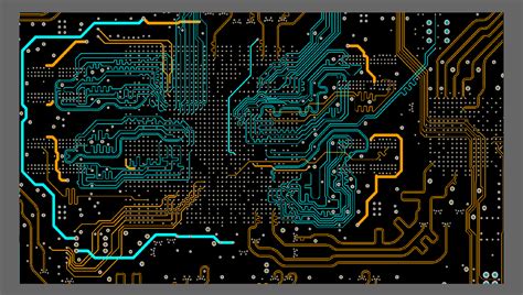
Introduction to PCB Drafting
Printed Circuit Board (PCB) drafting is a crucial step in the design and manufacture of electronic devices. It involves creating detailed drawings and schematics that accurately represent the layout, components, and connections of a PCB. Adhering to established drafting standards is essential to ensure clarity, consistency, and manufacturability of the final product.
In this article, we will explore five key drafting standards that every PCB designer should follow to create high-quality PCB drawings.
Importance of PCB Drafting Standards
Following PCB drafting standards offers several benefits:
-
Clarity and Readability: Standardized drawings are easier to understand and interpret by all stakeholders involved in the PCB design and manufacturing process.
-
Consistency: Adhering to a set of standards ensures consistency across different PCB designs, making it easier for manufacturers to work with various projects.
-
Error Reduction: By following established guidelines, designers can minimize the risk of errors and discrepancies in their drawings, leading to fewer issues during manufacturing.
-
Efficient Communication: Standardized drawings facilitate effective communication between designers, engineers, and manufacturers, reducing the likelihood of misinterpretation and delays.
-
Compliance: Many industries have specific requirements and regulations for PCB design and manufacture. Following drafting standards helps ensure compliance with these guidelines.

PCB Drafting Standard 1: Layer Stackup and Naming Conventions
Layer Stackup
The layer stackup is a critical aspect of PCB design, as it defines the arrangement and composition of the various layers within the board. A typical PCB consists of the following layers:
| Layer | Description |
|---|---|
| Top Layer | Contains components and routing |
| Ground Layer | Provides a ground reference plane |
| Power Layer | Distributes power to components |
| Signal Layers | Used for routing signals between components |
| Bottom Layer | Contains components and routing |
Designers should clearly specify the layer stackup in their PCB drawings, including the number of layers, their order, and their respective thicknesses.
Naming Conventions
Consistent naming conventions for layers, components, and nets are essential for clarity and organization. Some common naming conventions include:
- Layers: Use descriptive names such as “Top,” “Bottom,” “GND,” “PWR,” and “Signal1,” “Signal2,” etc.
- Components: Use a combination of the component type and a unique identifier, e.g., “R1” for resistor 1, “C2” for capacitor 2, etc.
- Nets: Use descriptive names that reflect the purpose of the net, e.g., “VCC” for power supply, “CLK” for clock signal, etc.
Adhering to a consistent naming convention throughout the PCB design process helps maintain clarity and reduces the risk of errors.

PCB Drafting Standard 2: Component Placement and Orientation
Component Placement
Proper component placement is crucial for optimizing PCB performance, manufacturability, and assembly. Consider the following guidelines:
-
Grouping: Place related components close together to minimize the length of traces and improve signal integrity.
-
Orientation: Orient components in a consistent direction to facilitate automated assembly processes and improve readability.
-
Clearance: Ensure sufficient clearance between components to allow for proper soldering and avoid interference.
-
Thermal Considerations: Place heat-generating components away from temperature-sensitive components to prevent thermal issues.
Component Orientation
Consistent component orientation enhances the readability of PCB drawings and simplifies the assembly process. Follow these guidelines:
-
Polarized Components: Orient polarized components (e.g., diodes, electrolytic capacitors) in a consistent direction, typically with the positive terminal on the left or top.
-
ICs: Orient ICs with pin 1 in a consistent location, usually in the top-left corner.
-
Connectors: Orient connectors with the mating side facing the edge of the board, unless otherwise specified.
-
Symmetry: If possible, maintain symmetry in component placement and orientation to improve the visual balance of the PCB.

PCB Drafting Standard 3: Routing and Trace Width
Routing Guidelines
Proper routing is essential for ensuring signal integrity and minimizing electromagnetic interference (EMI). Consider the following guidelines:
-
Trace Width: Select appropriate trace widths based on the current carrying requirements and the desired impedance of the signal.
-
Spacing: Maintain adequate spacing between traces to minimize crosstalk and EMI.
-
Routing Angles: Use 45-degree angles for trace routing to minimize reflections and improve signal integrity.
-
Via Placement: Place vias strategically to minimize the length of traces and improve signal quality.
Trace Width Considerations
The width of traces on a PCB is determined by several factors, including:
-
Current Carrying Capacity: Traces must be wide enough to safely carry the required current without excessive heating.
-
Impedance Control: Trace width, along with the thickness of the dielectric layer, affects the characteristic impedance of the trace.
-
Manufacturing Constraints: The minimum trace width is limited by the capabilities of the PCB manufacturing process.
Designers should consult the PCB manufacturer’s guidelines and use appropriate calculations to determine the optimal trace widths for their design.
PCB Drafting Standard 4: Silkscreen and Assembly Drawing
Silkscreen
The silkscreen layer on a PCB contains text and graphics that provide important information for assembly and identification. Consider the following guidelines:
-
Component Identification: Label components with their reference designators (e.g., R1, C2) to facilitate assembly and troubleshooting.
-
Polarity Marking: Clearly indicate the polarity of polarized components using symbols or text.
-
Fiducial Markers: Include fiducial markers on the silkscreen to assist with automated assembly alignment.
-
Text Size: Ensure that silkscreen text is legible and meets the manufacturer’s minimum size requirements.
Assembly Drawing
An assembly drawing provides a visual representation of the assembled PCB, including component placement and orientation. It serves as a guide for manual assembly and inspection. The assembly drawing should include:
-
Component Outlines: Show the outlines of all components, including their reference designators and values.
-
Orientation Indicators: Use clear orientation indicators (e.g., pin 1 markers) to ensure correct component placement.
-
Assembly Notes: Include any specific assembly instructions or precautions, such as torque requirements for fasteners.
-
Bill of Materials (BOM): Provide a complete BOM that lists all components used in the PCB assembly.
PCB Drafting Standard 5: Documentation and Revision Control
Documentation
Comprehensive documentation is essential for effective communication and collaboration throughout the PCB design and manufacturing process. PCB documentation should include:
-
Schematic Diagram: A detailed schematic that shows the electrical connections between components.
-
PCB Layout: The physical layout of the PCB, including component placement, routing, and layer stackup.
-
Bill of Materials (BOM): A complete list of all components used in the PCB assembly.
-
Assembly Instructions: Detailed instructions for assembling the PCB, including any special requirements or precautions.
Revision Control
Revision control is critical for tracking changes and ensuring that all stakeholders are working with the most up-to-date version of the PCB design. Implement the following practices:
-
Version Numbering: Use a consistent version numbering scheme (e.g., v1.0, v1.1) to identify different revisions of the PCB design.
-
Change Log: Maintain a change log that documents all modifications made to the PCB design, including the date, author, and a brief description of the changes.
-
Archive: Keep an archive of all previous versions of the PCB design files for reference and traceability.
-
Access Control: Implement access control measures to ensure that only authorized personnel can make changes to the PCB design files.
Frequently Asked Questions (FAQ)
-
Q: Why is it important to follow PCB drafting standards?
A: Following PCB drafting standards ensures clarity, consistency, and manufacturability of the final product. It reduces the risk of errors, facilitates effective communication, and helps maintain compliance with industry regulations. -
Q: What are the key considerations for component placement on a PCB?
A: When placing components on a PCB, consider grouping related components together, maintaining consistent orientation, ensuring sufficient clearance, and taking into account thermal considerations to optimize performance and manufacturability. -
Q: How do I determine the appropriate trace width for my PCB design?
A: The appropriate trace width depends on factors such as current carrying capacity, desired impedance, and manufacturing constraints. Consult the PCB manufacturer’s guidelines and use appropriate calculations to determine the optimal trace widths for your design. -
Q: What information should be included in the silkscreen layer of a PCB?
A: The silkscreen layer should include component identification (reference designators), polarity markings for polarized components, fiducial markers for automated assembly alignment, and legible text that meets the manufacturer’s minimum size requirements. -
Q: How can I effectively manage revisions of my PCB design?
A: To manage PCB design revisions effectively, implement a consistent version numbering scheme, maintain a change log, keep an archive of previous versions, and enforce access control measures to ensure that only authorized personnel can make changes to the design files.
Conclusion
Adhering to PCB drafting standards is essential for creating high-quality, manufacturable PCB designs. By following the five key standards outlined in this article – layer stackup and naming conventions, component placement and orientation, routing and trace width, silkscreen and assembly drawing, and documentation and revision control – PCB designers can ensure clarity, consistency, and compliance throughout the design and manufacturing process.
Investing time and effort into understanding and implementing these drafting standards will ultimately lead to more efficient workflows, fewer design iterations, and higher-quality PCB products. As the electronics industry continues to evolve, staying up-to-date with the latest drafting standards and best practices will be crucial for success in the field of PCB design.


Leave a Reply