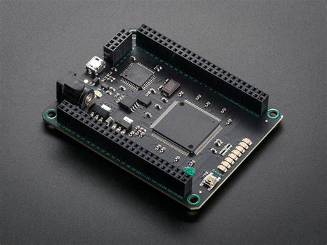
What is an FPGA Board?
An FPGA (Field-Programmable Gate Array) board is a versatile and powerful programmable logic device that allows developers to rapidly prototype and test digital circuits and systems. Unlike traditional integrated circuits that have fixed functionality, FPGAs can be reprogrammed and reconfigured after manufacturing, providing unparalleled flexibility and adaptability.
FPGAs consist of an array of configurable logic blocks (CLBs), interconnected through a programmable routing matrix. Each CLB contains a set of lookup tables (LUTs) and flip-flops that can be configured to implement various logical functions, such as AND, OR, and XOR gates, as well as more complex combinational and sequential circuits.
The programmable routing matrix enables the interconnection of CLBs, allowing designers to create complex digital systems by wiring together multiple logic blocks. This flexibility makes FPGAs suitable for a wide range of applications, from simple glue logic to high-performance computing, digital signal processing, and embedded systems.
Advantages of Using FPGA Boards for Rapid Prototyping
1. Flexibility and Reconfigurability
One of the primary advantages of using FPGA boards for rapid prototyping is their flexibility and reconfigurability. Unlike application-specific integrated circuits (ASICs), which have fixed functionality, FPGAs can be reprogrammed and reconfigured as needed, allowing designers to modify and optimize their designs throughout the development process.
This flexibility enables developers to quickly iterate on their designs, test various implementations, and make changes without incurring the high costs and long lead times associated with ASIC fabrication. As a result, FPGAs are ideal for prototyping and proof-of-concept development, where the ability to rapidly modify and refine designs is crucial.
2. Parallel Processing Capabilities
FPGAs offer significant advantages in terms of parallel processing capabilities compared to traditional microprocessors. While microprocessors execute instructions sequentially, FPGAs can perform multiple operations simultaneously, exploiting the inherent parallelism in many algorithms and applications.
This parallel processing capability makes FPGAs particularly well-suited for applications that require high-throughput data processing, such as digital signal processing, image and video processing, and network packet processing. By leveraging the parallel processing power of FPGAs, designers can achieve significant performance improvements and reduce latency compared to software-based implementations running on general-purpose processors.
3. Lower Development Costs and Faster Time-to-Market
Rapid prototyping with FPGA boards can significantly reduce development costs and accelerate time-to-market compared to traditional ASIC design flows. The reconfigurability of FPGAs allows designers to quickly test and validate their designs, identify and fix bugs, and make necessary modifications without incurring the high non-recurring engineering (NRE) costs associated with ASIC fabrication.
Moreover, FPGA development tools and frameworks have evolved to provide high-level design entry methods, such as hardware description languages (HDLs) like VHDL and Verilog, as well as high-level synthesis (HLS) tools that enable designers to describe their designs using high-level programming languages like C, C++, and SystemC. These tools abstract away many of the low-level details of FPGA Programming, making it easier and faster for developers to create and verify their designs.
4. Energy Efficiency
FPGAs can offer energy efficiency advantages over general-purpose processors in certain applications. By implementing custom hardware accelerators and optimizing designs for specific tasks, FPGAs can achieve higher performance per watt compared to software running on power-hungry CPUs.
This energy efficiency is particularly important in battery-powered and embedded systems, where power consumption is a critical concern. By offloading computationally intensive tasks to energy-efficient FPGA implementations, designers can extend battery life and reduce overall system power consumption.

FPGA Board Architecture and Components
A typical FPGA board consists of several key components that enable its programmability and functionality. Understanding these components is essential for effective FPGA-based rapid prototyping.
1. FPGA Chip
At the heart of an FPGA board is the FPGA chip itself. The FPGA chip contains the array of configurable logic blocks (CLBs) and the programmable routing matrix that allows designers to create custom digital circuits.
Modern FPGA chips also include a variety of specialized hardware resources, such as:
- Block RAM (BRAM): On-chip memory blocks that can be used for data storage, buffering, and caching.
- Digital Signal Processing (DSP) Slices: Dedicated hardware blocks optimized for digital signal processing operations, such as multiplication, addition, and accumulation.
- High-Speed I/O Transceivers: Specialized input/output blocks that support high-speed serial communication protocols, such as PCI Express, Ethernet, and SerDes.
- Phase-Locked Loops (PLLs) and Delay-Locked Loops (DLLs): Clock management and synchronization circuits that allow designers to generate and manipulate clock signals within the FPGA.
The specific mix and quantity of these hardware resources vary depending on the FPGA family and device, providing designers with a range of options to meet their application requirements.
2. Configuration Memory
FPGAs use configuration memory to store the bitstream that defines the functionality of the device. This memory is typically volatile, meaning that it loses its contents when power is removed. As a result, FPGAs must be reconfigured every time they are powered on.
There are several types of configuration memory used in FPGAs, including:
- SRAM: Static Random Access Memory is the most common type of configuration memory in FPGAs. SRAM is volatile, fast, and can be easily reprogrammed, making it well-suited for rapid prototyping and development.
- Flash: Some FPGAs use non-volatile flash memory for configuration storage, allowing the device to retain its configuration even when power is removed. This is useful for applications that require instant-on functionality or low power consumption.
- Antifuse: Antifuse-based FPGAs are programmed by permanently “burning” connections between logic blocks, creating a one-time-programmable (OTP) device. While antifuse FPGAs offer high security and reliability, they are less flexible than SRAM or flash-based devices.
3. I/O Interfaces
FPGA boards include a variety of input/output (I/O) interfaces that allow the device to communicate with external systems and peripherals. These interfaces can include:
- General-Purpose I/O (GPIO) Pins: Configurable pins that can be used for simple digital input and output, such as buttons, switches, and LEDs.
- Memory Interfaces: Dedicated interfaces for connecting external memory devices, such as SDRAM, DDR, and SRAM.
- Communication Interfaces: High-speed serial interfaces, such as USB, Ethernet, and PCI Express, for communicating with other systems and devices.
- Analog Interfaces: Some FPGA boards include analog-to-digital converters (ADCs) and digital-to-analog converters (DACs) for interfacing with analog signals.
The specific mix of I/O interfaces available on an FPGA board depends on the intended application and the target market for the device.

FPGA Design Flow and Tools
The FPGA design flow involves several steps and tools that enable designers to create, simulate, and implement their designs on an FPGA board.
1. Design Entry
The first step in the FPGA design flow is design entry, where designers describe the functionality of their system using a hardware description language (HDL) or a high-level synthesis (HLS) tool.
HDLs, such as VHDL and Verilog, allow designers to describe the behavior and structure of digital circuits using a textual format. HDLs provide a level of abstraction above the physical implementation, enabling designers to focus on the functionality of their system rather than the low-level details of the FPGA architecture.
HLS tools, such as Xilinx Vivado HLS and Intel OpenCL HLS, allow designers to describe their designs using high-level programming languages like C, C++, and SystemC. HLS tools automatically generate synthesizable HDL code from the high-level description, reducing the time and effort required to create FPGA designs.
2. Simulation and Verification
Once the design has been entered using an HDL or HLS tool, the next step is to simulate and verify its functionality. Simulation allows designers to test their designs in a virtual environment, ensuring that the system behaves as expected before committing to hardware.
There are two main types of simulation used in FPGA design:
- Behavioral Simulation: Also known as functional simulation, behavioral simulation verifies the logic and functionality of the design without considering timing information. This type of simulation is fast and useful for catching logical errors early in the design process.
- Timing Simulation: Timing simulation takes into account the propagation delays of the FPGA’s physical resources, providing a more accurate representation of the design’s behavior under real-world conditions. Timing simulation is essential for ensuring that the design meets its performance requirements and constraints.
In addition to simulation, designers may also use formal verification techniques, such as equivalence checking and property checking, to mathematically prove the correctness of their designs.
3. Synthesis
After the design has been verified through simulation, the next step is synthesis. Synthesis is the process of transforming the HDL or HLS description into a gate-level netlist, which represents the design in terms of the FPGA’s physical resources (CLBs, LUTs, flip-flops, etc.).
The synthesis tool optimizes the design for the target FPGA architecture, applying various techniques such as logic minimization, resource sharing, and technology mapping to create an efficient implementation.
4. Place and Route
The place and route step takes the synthesized netlist and maps it onto the physical resources of the FPGA. The placer determines the optimal location for each logic element, while the router connects these elements using the FPGA’s programmable routing matrix.
The place and route process is guided by user-defined constraints, such as timing requirements, power constraints, and pin assignments. The tool iteratively refines the placement and routing to meet these constraints, optimizing the design for performance, power, and area.
5. Bitstream Generation and Programming
Once the design has been placed and routed, the final step is to generate a bitstream, which is a binary file that contains the configuration data for the FPGA. The bitstream is used to program the FPGA’s configuration memory, defining the functionality of the device.
Most FPGA boards include a configuration interface, such as JTAG or SelectMAP, which allows the bitstream to be loaded into the device. Some boards also support on-board configuration memory, such as flash or EEPROM, enabling the FPGA to be automatically configured on power-up.

Applications of FPGA Boards in Rapid Prototyping
FPGA boards are widely used for rapid prototyping in various domains, ranging from consumer electronics to aerospace and defense. Some common applications include:
1. Digital Signal Processing
FPGAs are well-suited for digital signal processing (DSP) applications, such as audio and video processing, radar signal processing, and wireless communication. The parallel processing capabilities and dedicated DSP resources in modern FPGAs enable high-performance, low-latency processing of real-time signals.
Rapid prototyping with FPGA boards allows DSP designers to quickly implement and test their algorithms, optimize their designs for performance and power, and verify functionality before committing to a final implementation.
2. Embedded Systems
FPGAs are increasingly used in embedded systems, where they can provide a flexible and efficient alternative to traditional microcontrollers and processors. By implementing custom hardware accelerators and peripherals, FPGAs can offload computationally intensive tasks from the main processor, reducing power consumption and improving overall system performance.
Rapid prototyping with FPGA boards enables embedded system designers to quickly develop and test their designs, integrate custom peripherals, and optimize their systems for specific applications.
3. Aerospace and Defense
FPGAs are widely used in aerospace and defense applications, where they offer high performance, reliability, and flexibility. Rapid prototyping with FPGA boards allows designers to create and test complex systems, such as radar processing, satellite communication, and avionics, in a shorter timeframe compared to traditional design methods.
The reprogrammability of FPGAs is particularly beneficial in aerospace and defense applications, as it allows for in-field updates and modifications to adapt to changing requirements and threats.
4. Automotive
The automotive industry is increasingly adopting FPGAs for rapid prototyping and production systems. FPGAs are used in various automotive applications, such as advanced driver assistance systems (ADAS), infotainment systems, and engine control units (ECUs).
Rapid prototyping with FPGA boards enables automotive designers to quickly develop and test new features, optimize their designs for performance and power, and ensure compliance with strict safety and reliability standards.
FPGA Board Prototyping Platforms and Ecosystems
There are several FPGA board prototyping platforms and ecosystems available, each offering different features, tools, and support. Some popular platforms include:
1. Xilinx
Xilinx is one of the leading FPGA manufacturers, offering a wide range of FPGA boards and development tools. The Xilinx ecosystem includes:
- Vivado Design Suite: A comprehensive design environment for Xilinx FPGAs, including tools for design entry, synthesis, simulation, and implementation.
- Vitis Unified Software Platform: An integrated development environment for software, hardware, and AI acceleration, supporting high-level languages like C, C++, and Python.
- Xilinx Evaluation Boards: A range of FPGA boards for prototyping and development, such as the Artix, Kintex, and Virtex series.
2. Intel
Intel, through its acquisition of Altera, offers a comprehensive FPGA platform for rapid prototyping and development. The Intel FPGA ecosystem includes:
- Quartus Prime Design Software: A complete design environment for Intel FPGAs, including tools for design entry, synthesis, simulation, and implementation.
- OpenCL SDK for FPGAs: A high-level programming model for accelerating algorithms on Intel FPGAs using the OpenCL standard.
- Intel FPGA Development Kits: A range of FPGA boards for prototyping and development, such as the Cyclone, Arria, and Stratix series.
3. Microsemi
Microsemi, a subsidiary of Microchip Technology, offers a range of FPGA boards and development tools for rapid prototyping and deployment. The Microsemi ecosystem includes:
- Libero SoC Design Suite: A comprehensive design environment for Microsemi FPGAs, including tools for design entry, synthesis, simulation, and implementation.
- SoftConsole IDE: An integrated development environment for embedded software development on Microsemi FPGAs.
- Microsemi FPGA Development Kits: A range of FPGA boards for prototyping and development, such as the PolarFire and SmartFusion2 series.
Choosing the right FPGA board prototyping platform depends on factors such as performance requirements, power constraints, available resources, and familiarity with the tools and ecosystem.
Table: Comparison of Popular FPGA Board Prototyping Platforms
| Platform | FPGA Families | Design Tools | High-Level Synthesis | Key Features |
|---|---|---|---|---|
| Xilinx | Artix, Kintex, Virtex, Zynq | Vivado Design Suite, Vitis | Vivado HLS, Vitis HLS | Extensive IP library, AI acceleration, adaptive compute acceleration |
| Intel | Cyclone, Arria, Stratix | Quartus Prime, OpenCL SDK | OpenCL HLS | High-performance DSP, Hyperflex architecture, advanced power management |
| Microsemi | PolarFire, SmartFusion2 | Libero SoC, SoftConsole | Libero SoC SmartDesign | Low power, security, reliability, mixed-signal integration |
Best Practices for Rapid Prototyping with FPGA Boards
To make the most of rapid prototyping with FPGA boards, consider the following best practices:
-
Start with a clear set of requirements and constraints for your design, including performance targets, power budget, and I/O interfaces.
-
Choose an FPGA board and development platform that aligns with your requirements and your team’s expertise.
-
Use version control systems to manage your HDL code, constraints, and project files, enabling collaboration and trackability.
-
Leverage high-level synthesis tools and IP libraries to accelerate your design process and focus on system-level functionality.
-
Perform thorough simulation and verification at each stage of the design process to catch bugs early and ensure correctness.
-
Optimize your design for the target FPGA architecture, considering factors such as resource utilization, timing, and power consumption.
-
Document your design thoroughly, including design decisions, constraints, and test procedures, to facilitate future maintenance and modifications.
Frequently Asked Questions (FAQ)
Q1: What is the difference between an FPGA and a microprocessor?
A1: FPGAs and microprocessors serve different purposes and have distinct architectures. A microprocessor is a fixed-architecture device that executes instructions sequentially, while an FPGA is a programmable logic device that can be configured to implement custom hardware circuits and execute multiple operations


Leave a Reply