What is a PCB?
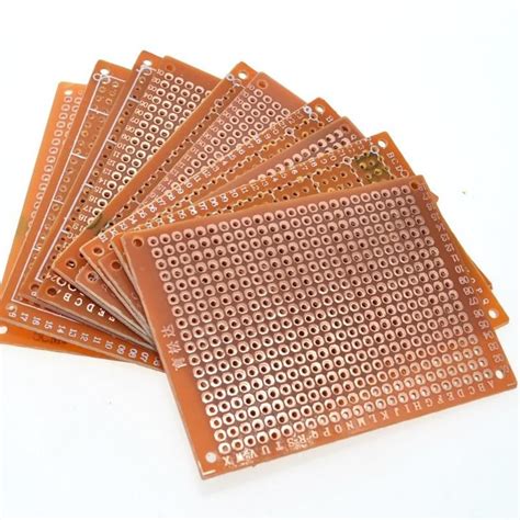
A Printed Circuit Board, or PCB, is a flat board made of insulating material, such as fiberglass or plastic, with conductive copper traces printed on its surface. These traces connect various electronic components, like resistors, capacitors, and integrated circuits (ICs), to create a functional electronic circuit. PCBs are used in almost all electronic devices, from smartphones and computers to home appliances and industrial equipment.
Why Make Your Own PCB?
There are several reasons why you might want to create your own PCB:
-
Cost-effectiveness: Making your own PCB can be cheaper than buying a pre-made one, especially if you need multiple copies or have a custom design.
-
Customization: When you make your own PCB, you have complete control over the design, layout, and components used. This allows you to tailor the board to your specific needs and requirements.
-
Learning experience: Creating a DIY PCB is an excellent way to learn about electronics and gain hands-on experience with circuit design and fabrication.
-
Rapid prototyping: Making your own PCB enables you to quickly test and refine your designs, reducing the time and cost associated with outsourcing prototype fabrication.
Tools and Materials Required
To create your own PCB, you’ll need the following tools and materials:
- Copper-clad board (single or double-sided)
- Etch-resistant marker or transfer paper
- PCB design software (e.g., KiCad, Eagle, or EasyEDA)
- Laser printer (for toner transfer method)
- Laminator (optional, for toner transfer method)
- Ferric chloride or other PCB etchant
- Plastic container for etching
- Drill or drill press
- Safety equipment (gloves, goggles, and protective clothing)
- Soldering iron and solder
- Isopropyl alcohol for cleaning

Designing Your PCB
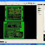
The first step in creating your DIY PCB is to design the circuit. You can use PCB design software like KiCad, Eagle, or EasyEDA to create a schematic diagram and lay out the components on the board. These software tools are available for free or have affordable licensed versions, and they offer extensive libraries of components and footprints.
When designing your PCB, consider the following factors:
- Component placement: Arrange components in a logical and efficient manner to minimize the length of traces and reduce the risk of interference.
- Trace width: Ensure that the traces are wide enough to handle the expected current flow without overheating or causing voltage drops.
- Ground plane: Include a ground plane to reduce electromagnetic interference and improve signal integrity.
- Mounting holes: Add mounting holes to secure the PCB in place.
Once you have completed the design, generate Gerber files, which are the standard format for PCB fabrication.
PCB Fabrication Methods
There are several methods for fabricating a PCB at home, each with its own advantages and disadvantages. We’ll focus on two of the most popular methods: the toner transfer method and the photoresist method.
Toner Transfer Method
The toner transfer method involves printing the PCB layout onto a special transfer paper using a laser printer, then transferring the toner onto the copper-clad board using heat and pressure.
-
Print the PCB layout onto the transfer paper using a laser printer. Make sure to mirror the image so that it appears correctly on the final board.
-
Clean the copper-clad board with isopropyl alcohol to remove any grease or debris.
-
Place the transfer paper onto the copper side of the board, with the toner facing down.
-
Use a laminator or a household iron to apply heat and pressure evenly across the paper. This will transfer the toner onto the copper surface.
-
Allow the board to cool, then carefully peel off the transfer paper. The toner should have adhered to the copper, creating an etch-resistant mask.
Photoresist Method
The photoresist method involves applying a light-sensitive photoresist to the copper-clad board, exposing it to UV light through a transparency of the PCB layout, and then developing the resist to create an etch-resistant mask.
-
Clean the copper-clad board with isopropyl alcohol.
-
Apply a thin, even layer of photoresist to the copper surface using a pre-sensitized board or liquid photoresist.
-
Allow the photoresist to dry completely.
-
Print the PCB layout onto a transparency using a laser printer or inkjet printer with transparency film.
-
Place the transparency onto the photoresist-coated board, with the ink side facing down.
-
Expose the board to UV light for the recommended time, which varies depending on the type of photoresist used.
-
Develop the photoresist using the appropriate developer solution, following the manufacturer’s instructions. The unexposed areas will dissolve, leaving an etch-resistant mask.
Etching the PCB
Once you have created the etch-resistant mask using either the toner transfer or photoresist method, it’s time to etch the PCB.
-
Prepare the etching solution according to the manufacturer’s instructions. Ferric chloride is a common etchant, but there are also less toxic alternatives available.
-
Place the PCB into the etching solution, ensuring that it is fully submerged.
-
Agitate the solution gently to ensure even etching. The etching process typically takes 10-30 minutes, depending on the strength of the solution and the thickness of the copper.
-
Periodically check the PCB to monitor the etching progress. Remove the board from the solution once all the unwanted copper has been etched away.
-
Rinse the PCB thoroughly with water and remove the etch-resistant mask using isopropyl alcohol or acetone.
Drilling and Soldering
After etching, you’ll need to drill holes for through-hole components and solder the components onto the board.
-
Use a drill or drill press to create holes at the appropriate locations on the PCB. Ensure that the drill bit size matches the component leads.
-
Clean the PCB with isopropyl alcohol to remove any debris.
-
Insert the component leads through the corresponding holes on the PCB.
-
Solder the components in place using a soldering iron and solder. Be sure to use the appropriate soldering technique and avoid creating solder bridges between adjacent pads.
-
Inspect the soldered joints for any defects or cold solder joints, and re-solder if necessary.
Testing and Troubleshooting
Once you have assembled your PCB, it’s essential to test it to ensure that it functions as intended.
-
Visually inspect the board for any obvious defects, such as solder bridges, unsoldered components, or damaged traces.
-
Use a multimeter to check for continuity between the appropriate points on the board.
-
Apply power to the board and measure the voltage levels at various points to ensure they match the expected values.
-
Test the functionality of the circuit by connecting any necessary inputs and outputs and verifying the desired behavior.
If you encounter any issues during testing, troubleshoot the board by:
- Double-checking the component placement and orientation
- Inspecting solder joints for any defects or cold solder joints
- Verifying that the PCB layout matches the schematic diagram
- Checking for any damaged or shorted traces
PCB Design and Fabrication Tips
To ensure the best results when creating your DIY PCB, consider the following tips:
-
Keep it simple: When starting out, design simple circuits with fewer components to minimize the risk of errors and make troubleshooting easier.
-
Plan your layout: Carefully plan the component placement and routing to minimize the length of traces and reduce the risk of interference.
-
Use a grid: When laying out components and traces, use a grid to ensure proper alignment and spacing.
-
Double-check your design: Before fabricating your PCB, double-check the schematic diagram and PCB layout for any errors or inconsistencies.
-
Test your toner transfer: If using the toner transfer method, test the transfer process on a scrap piece of copper-clad board to ensure that the toner adheres properly.
-
Use fresh etchant: Always use fresh etching solution to ensure consistent and efficient etching.
-
Wear safety equipment: When handling chemicals and solder, always wear gloves, goggles, and protective clothing to ensure your safety.
FAQ
-
Can I make a multi-layer PCB at home?
Making multi-layer PCBs at home can be challenging and requires additional equipment and materials. It’s recommended to start with single-layer or double-sided PCBs as a beginner. -
What is the best software for designing PCBs?
There are several popular PCB design software options, including KiCad, Eagle, and EasyEDA. The best choice depends on your specific needs, experience level, and budget. -
Can I use an inkjet printer for the toner transfer method?
While it’s possible to use an inkjet printer for the toner transfer method, the results may not be as consistent or reliable as using a laser printer. Laser printers produce a thicker and more durable toner layer that adheres better to the copper surface. -
What should I do if the etchant is not removing the copper?
If the etchant is not removing the copper, it may be too weak or the etching process may not be taking place at the optimal temperature. Try using fresh etchant, increasing the temperature slightly, or agitating the solution more frequently. Also, ensure that the etch-resistant mask is fully covering the desired copper traces. -
How can I improve the quality of my soldered joints?
To improve the quality of your soldered joints, ensure that the soldering iron is at the proper temperature, use a high-quality solder, and apply the appropriate amount of solder to the joint. Keep the soldering iron tip clean and tinned, and avoid touching the joint with the iron for too long to prevent overheating or damaging the components.
Conclusion
Creating your own DIY PCB board can be a fun and rewarding experience for beginners in electronics. By following the steps outlined in this guide and using the appropriate tools and materials, you can design, fabricate, and assemble your own custom PCB at home. Remember to start with simple designs, take the necessary safety precautions, and be patient when troubleshooting any issues.
As you gain more experience and confidence in making your own PCBs, you can explore more advanced techniques, such as multi-layer boards or surface-mount components. With practice and persistence, you’ll be able to create professional-quality PCBs for your projects and prototypes.
| Method | Advantages | Disadvantages |
|---|---|---|
| Toner Transfer | – Inexpensive equipment – Quick and simple process |
– Transfer quality may vary – Limited to laser printer toner |
| Photoresist | – High-quality, consistent results – Suitable for fine details and traces |
– Requires additional equipment and materials – More time-consuming process |
| Component Type | Soldering Tip |
|---|---|
| Through-hole | – Use a larger soldering iron tip – Apply solder to both the component lead and the pad |
| Surface-mount | – Use a fine-tipped soldering iron – Apply a small amount of solder to the pad, then position the component and solder in place |
By mastering the art of DIY PCB fabrication, you’ll open up a world of possibilities for your electronics projects and gain a deeper understanding of the principles behind circuit design and manufacturing.
Leave a Reply