What is a PCB?
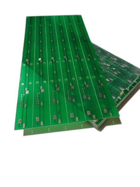
A PCB, or printed circuit board, is the foundation of most electronic devices. It’s a flat board made of insulating material like fiberglass, with conductive copper traces printed on it in a specific pattern. Electronic components like resistors, capacitors, and integrated circuits are then soldered onto the PCB to create a functional circuit.
PCBs offer several advantages over point-to-point wiring or breadboard circuits:
- Compact size
- Improved reliability
- Easier mass production
- Better noise immunity
- More professional appearance
PCB fabrication Process Overview
The basic steps to make a PCB at home are:
- Design the circuit schematic
- Create the PCB layout
- Print the layout onto a transparency
- Transfer the layout to a copper clad board
- Etch away the unwanted copper
- Drill holes for components
- Solder on the components
We’ll go through each of these steps in detail.
Tools and Materials Needed
Before you get started, gather the following tools and materials:
- Computer with PCB design software
- Laser printer
- Transparency film
- Copper clad board
- Ferric chloride etching solution
- Plastic tray for etching
- Rubber gloves and safety goggles
- Fine grit sandpaper
- Drill with small bits
- Soldering iron and solder
You can find most of these items at electronics hobby shops or online retailers.

Step 1: Design the Circuit Schematic
The first step in making a PCB is to design your circuit schematic using PCB design software. Some popular options are:
- KiCad (free and open source)
- EAGLE (free for small boards)
- EasyEDA (online, free)
- Altium Designer (paid)
If you’re a beginner, start with a simple circuit like a LED flasher or audio amplifier. Find an existing schematic online or in a electronics magazine and recreate it in the software.
The schematic captures the electrical connections between components, but not the physical layout. Make sure to:
- Add all the necessary components
- Make the right connections between components
- Specify component values
- Label key nodes
- Run electrical rule checks
Step 2: Create the PCB Layout
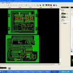
With the completed schematic, you can now design the physical PCB layout in the software. The layout editor lets you arrange components and route the copper traces that connect them.
General PCB layout guidelines:
- Keep trace lengths as short as possible
- Make traces wider for higher current
- Avoid 90 degree trace corners
- Leave enough space between components
- Have a good ground plane
- Keep sensitive analog and digital circuits separate
Your PCB design software will have tools to help you comply with design rules and catch errors. Do a design rule check before finalizing the layout.
Step 3: Print the Layout
Once you’re happy with the PCB layout, print it out at actual size (1:1 scale) on a transparency film using a laser printer. You may need to flip or mirror the layout so it prints correctly for the transfer process.
Print on the glossy side of the transparency. For best results, print two copies and stack them to get a darker, more opaque image.
Cut out the printed layout with a scissors, leaving some margin around the edges of the board outline.
Step 4: Transfer Layout to Copper Board
Now you’ll transfer the printed layout to a copper clad board. The copper board has a thin layer of copper bonded to an insulating substrate like fiberglass.
Cut a piece of copper board to the size of your layout using a saw or cutting shears. Clean the copper surface with fine sandpaper and wipe it down with alcohol to remove any dirt and oils.
Place the transparency with the printed layout toner-side down on the copper board. Carefully align it and tape down the edges with heat resistant tape.
Apply heat and pressure to the transparency and board using a laminator or a clothes iron set to high temperature (no steam). This melts the toner and fuses it to the copper surface.
After heating for a few minutes, let the board cool down. Then peel off the transparency slowly, making sure all the toner sticks to the copper. Touch up any missing spots with a permanent marker.
The PCB layout pattern should now be clearly visible on the copper board, with the toner acting as an etch resist.
Step 5: Etch the Copper Board
The next step is to chemically etch away all the unwanted copper, leaving only your circuit traces behind. The most common chemical etchant used is ferric chloride, which is available premixed or as a powder you mix with water.
Pour the ferric chloride solution into a plastic tray. Put on rubber gloves and safety goggles. Carefully place your copper board, layout side up, into the solution.
Gently agitate the tray so the solution flows over the board. You should see the copper starting to dissolve where it’s not covered by toner. The etching process can take 15-45 minutes depending on the solution strength and temperature.
Periodically check on the etching progress. When all the unwanted copper is gone, remove the board and rinse it thoroughly with water.
The board should now have copper traces matching your circuit layout, with the rest of the substrate exposed. Strip off the toner etch resist with acetone or alcohol to reveal the final copper traces.
Step 6: Drill Holes and Cut Out Board
Most PCB components are through-hole parts that get soldered on the opposite side from the traces. So you’ll need to drill holes for the component leads at each pad location.
Put the etched board over a piece of scrap wood. Use a drill press or a handheld drill with a small bit (0.7-1mm) to carefully drill a hole at each pad.
Use a larger bit for any mounting holes or vias that connect the top and bottom copper layers.
After drilling all the holes, cut out the final board shape using a saw or nibbling tool. Cut right along the board outline you etched.
Sand the edges smooth with sandpaper or a file. Your PCB is now ready for components!
Step 7: Solder Components
The final assembly step is to solder the components onto the PCB. Follow the layout diagram for placing components.
Bend the component leads and insert them through the holes. Resistors and capacitors can go either way, but polarized parts like diodes and electrolytic caps must go the right direction. Integrated circuits often have a notch or dot indicating pin 1.
Flip the board over and solder each component lead to its copper pad. Heat up both the lead and pad with the soldering iron, then apply solder until it flows around the joint. Snip off the excess lead with wire cutters.
Some tips for good soldering:
- Use thin solder and a clean, tinned soldering iron tip
- Apply heat to both the component lead and PCB pad
- Don’t apply the solder directly to the iron
- Make sure the joint is shiny and cone-shaped
- Avoid bridging solder between adjacent pads
- Clean the iron tip frequently on a wet sponge
Once all the components are soldered, visually inspect the joints for good connections. Use a multimeter to check for continuity and shorts.
And there you have it – a completed, custom PCB made in your own workshop! Power it up and test out your circuit.
Frequently Asked Questions
What is the best free PCB design software for beginners?
Two good free options for PCB design software are KiCad and EAGLE. KiCad is open source, while EAGLE has a free license that supports boards up to 80cm2.
What’s the thinnest copper clad board I can use?
Common PCB copper thicknesses are 1 oz (35 μm) and 2 oz (70 μm). 1 oz copper is thinner and easier to etch but can’t handle as much current as 2 oz. For beginners, 1 oz is a good place to start.
How long does it take to etch a PCB?
The etching time depends on the solution type, strength, and temperature, as well as the size of your board. For a typical 4×6″ board in fresh ferric chloride, it may take 15-45 minutes. You can speed it up by heating the solution.
Do I need to use a ground plane on my PCB?
A ground plane is a large copper area on the PCB tied to ground. While not strictly necessary, a ground plane has benefits like lower noise, better power supply decoupling, and reduced loop area. It’s a good idea to use one if you have space.
How small of a PCB trace can I make at home?
The minimum trace width depends on your etching process and drill size. For manual etching, 0.5-1mm (20-40 mils) is a reliably achievable trace width and spacing for most beginners. Traces for high current should be wider.
Summary
Making your own PCBs at home is a great way to prototype circuits and bring your electronic projects to life. With some low-cost materials, basic tools, and a methodical process, you can design and fabricate custom PCBs for your devices.
The key steps are designing the circuit schematic, creating the PCB layout, transferring the layout to copper board, etching away excess copper, drilling holes, and soldering components. While it takes some practice to get reliable results, the satisfaction of using your own homemade PCBs is well worth the effort.
Just remember to always work safely, follow good PCB layout principles, and test your boards carefully. Get creative and have fun expressing your circuits as PCBs!
| Material/Tool | Purpose |
|---|---|
| PCB design software | Create circuit schematic and board layout |
| Laser printer | Print layout onto transparency |
| Transparency film | Transfer printed layout to copper board |
| Copper clad board | Substrate for etching circuit traces |
| Ferric chloride | Etchant to dissolve unwanted copper |
| Drill and bits | Make holes for component leads and vias |
| Soldering iron and solder | Attach components to PCB pads |
I hope this article provides a helpful overview of the process of making your own PCBs at home. Let me know if you have any other questions!
Leave a Reply