What is AD-to-Gerber Conversion?
AD-to-Gerber conversion is the process of translating Altium Designer (AD) files into a format that can be used by manufacturing facilities to produce printed circuit boards (PCBs). Gerber files are the industry standard for PCB manufacturing, and they contain all the necessary information for fabricating the board, including copper layers, solder mask, silkscreen, and drill data.
Why Convert AD Files to Gerber?
Converting AD files to Gerber is essential for several reasons:
-
Manufacturing Compatibility: Most PCB manufacturing facilities require Gerber files as input for their production processes. By converting your AD files to Gerber, you ensure that your design can be manufactured by a wide range of fabricators.
-
Standardization: Gerber files provide a standardized format for PCB data, which helps to avoid misinterpretation or errors during the manufacturing process.
-
Quality Control: Generating Gerber files allows you to review your design in a format that closely represents the final manufactured product, enabling you to catch any errors or discrepancies before sending the files to the manufacturer.
Prerequisites for AD-to-Gerber Conversion
Before you begin the AD-to-Gerber conversion process, ensure that you have the following:
-
Altium Designer Software: You’ll need a licensed version of Altium Designer to open and work with your PCB design files.
-
Completed PCB Design: Your PCB design should be finalized and ready for manufacturing. This includes ensuring that all components are placed, routed, and free of design rule violations.
-
Layer Stack-up Definition: Define your PCB’s layer stack-up, which includes the number of layers, their order, and the materials used for each layer. This information is crucial for generating accurate Gerber files.
Step-by-Step Guide to AD-to-Gerber Conversion
Follow these steps to convert your AD files to Gerber:
Step 1: Open Your PCB Design in Altium Designer
Launch Altium Designer and open your PCB design project.
Step 2: Define the Layer Stack-up
- In the PCB editor, go to “Design” > “Layer Stack Manager.”
- Define your layer stack-up, specifying the number of layers, their order, and the materials used for each layer.
- Click “OK” to save the layer stack-up.
Step 3: Configure Gerber Output Settings
- Go to “File” > “Fabrication Outputs” > “Gerber Files.”
- In the Gerber Setup dialog box, configure the following settings:
- Format: Choose “RS-274X” for extended Gerber format.
- Units: Select “Metric” or “Imperial” based on your design requirements.
- Coordinate Format: Choose the appropriate coordinate format (e.g., 4.5, 4.6) based on the precision required for your design.
- Aperture Format: Select “Embedded aperture” to include aperture definitions within the Gerber files.
- Click “OK” to save the settings.
Step 4: Generate Gerber Files
- In the Gerber Setup dialog box, click “Export All.”
- Choose a destination folder for the generated Gerber files.
- Click “OK” to start the Gerber file generation process.
Step 5: Review and Verify Gerber Files
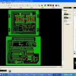
- Open the generated Gerber files using a Gerber viewer software (e.g., GC-Prevue, ViewMate).
- Carefully review each layer to ensure that the design is accurate and complete.
- Check for any missing or incorrect features, such as pads, traces, or drill holes.
- Verify that the Gerber files match your intended design and layer stack-up.
Step 6: Package and Send Gerber Files to Manufacturer
- Create a compressed archive (e.g., ZIP) containing all the generated Gerber files.
- Include any additional files required by the manufacturer, such as drill files, solder paste files, or assembly drawings.
- Send the packaged Gerber files to your chosen PCB manufacturer for fabrication.

Common Gerber File Extensions and Their Meanings
When generating Gerber files, you’ll encounter various file extensions that correspond to different layers and aspects of your PCB design. Here are some common Gerber file extensions and their meanings:
| Extension | Layer/Aspect |
|---|---|
| .GTL | Top Copper Layer |
| .GBL | Bottom Copper Layer |
| .G1 – .Gn | Inner Copper Layers (n represents the layer number) |
| .GTO | Top Overlay (Silkscreen) |
| .GBO | Bottom Overlay (Silkscreen) |
| .GTS | Top Solder Mask |
| .GBS | Bottom Solder Mask |
| .GTP | Top Paste Mask |
| .GBP | Bottom Paste Mask |
| .TXT | Drill File (NC Drill) |
| .GM1 | Board Outline/Mechanical Layer |
Understanding these file extensions will help you identify and manage the various Gerber files generated during the AD-to-Gerber conversion process.
Tips for Successful AD-to-Gerber Conversion
-
Ensure Design Completeness: Before starting the conversion process, double-check that your PCB design is complete, and all components are properly placed, routed, and free of design rule violations.
-
Use Consistent Units: Maintain consistency in units throughout your design and Gerber output settings to avoid scaling issues during manufacturing.
-
Verify Layer Stack-up: Ensure that your layer stack-up definition matches your design requirements and is correctly configured in Altium Designer.
-
Review Gerber Files: Always review the generated Gerber files using a Gerber viewer to catch any errors or discrepancies before sending them to the manufacturer.
-
Communicate with Manufacturer: Consult with your chosen PCB manufacturer for their specific Gerber file requirements, such as file naming conventions, additional files needed, or preferred settings.
Frequently Asked Questions (FAQ)
-
What is the difference between Gerber and NC Drill files?
Gerber files contain information about the copper layers, solder mask, and silkscreen of a PCB, while NC Drill files contain information about the location, size, and type of drill holes required for the board. -
Can I generate Gerber files from other PCB design software besides Altium Designer?
Yes, most PCB design software, such as KiCad, Eagle, and OrCAD, have the capability to generate Gerber files. However, the specific steps and settings may vary depending on the software. -
What should I do if my manufacturer reports issues with my Gerber files?
If your manufacturer reports issues with your Gerber files, first verify that you have followed their specific requirements and guidelines. Review your Gerber files for any errors or discrepancies, and regenerate the files if necessary. If the issue persists, consult with your manufacturer for further guidance. -
How do I ensure that my Gerber files are compatible with my manufacturer’s requirements?
To ensure compatibility, communicate with your manufacturer and ask for their specific Gerber file requirements, such as file naming conventions, required layers, and preferred settings. Provide them with a sample set of Gerber files for review before finalizing your design. -
What are the benefits of using a Gerber viewer?
A Gerber viewer allows you to visually inspect your generated Gerber files, helping you to catch any errors, missing features, or discrepancies before sending the files to the manufacturer. This can save time and cost by avoiding unnecessary revisions and manufacturing delays.
Conclusion
AD-to-Gerber conversion is a critical step in the PCB design process, enabling you to translate your Altium Designer files into a format that can be used by manufacturing facilities. By following the steps outlined in this guide and adhering to best practices, you can ensure that your Gerber files are accurate, complete, and compatible with your chosen manufacturer’s requirements.
Remember to always review your Gerber files using a Gerber viewer, communicate with your manufacturer for specific guidelines, and maintain consistency throughout your design and output settings. By doing so, you’ll streamline the PCB fabrication process and minimize the risk of errors or delays.
As you become more familiar with AD-to-Gerber conversion, you’ll develop a better understanding of the various file extensions, settings, and requirements involved. This knowledge will enable you to create high-quality PCB designs that can be efficiently manufactured, bringing your electronic projects to life.


Leave a Reply