Introduction to PCB Etching
PCB etching is a critical process in the manufacturing of printed circuit boards (PCBs). It involves the removal of unwanted copper from the surface of the PCB substrate, leaving behind the desired conductive traces that form the electrical connections of the circuit. The quality of the etching process directly affects the functionality, reliability, and appearance of the final PCB.
In this comprehensive guide, we will delve into the various aspects of PCB etching, including the different methods, materials, and techniques used to achieve the perfect PCB etching results. Whether you are a hobbyist or a professional, understanding the intricacies of PCB etching is essential for creating high-quality PCBs.
Types of PCB Etching Methods
There are several methods used for PCB etching, each with its own advantages and disadvantages. Let’s explore the most common PCB etching methods:
1. Chemical Etching
Chemical etching is the most widely used method for PCB etching. It involves the use of a chemical etchant solution to remove the unwanted copper from the PCB substrate. The PCB is immersed in the etchant solution, which selectively dissolves the exposed copper while leaving the desired conductive traces intact.
Advantages of Chemical Etching
- Widely available and cost-effective
- Suitable for both small-scale and large-scale production
- Provides good control over the etching process
Disadvantages of Chemical Etching
- Requires handling of hazardous chemicals
- Proper disposal of etchant solution is necessary
- Can be time-consuming for complex designs
2. Laser Etching
Laser etching is a precise and advanced method for PCB etching. It utilizes a high-powered laser beam to vaporize the unwanted copper from the PCB substrate. The laser is guided by a computer-controlled system, allowing for highly accurate and intricate etching patterns.
Advantages of Laser Etching
- High precision and accuracy
- Suitable for complex designs and fine features
- Fast and efficient process
Disadvantages of Laser Etching
- Requires specialized equipment and expertise
- Higher initial investment compared to chemical etching
- Limited to certain PCB materials
3. Mechanical Etching
Mechanical etching involves the use of abrasive materials or tools to physically remove the unwanted copper from the PCB substrate. This method is less common compared to chemical and laser etching but can be useful in certain situations.
Advantages of Mechanical Etching
- Does not require hazardous chemicals
- Can be used for selective etching or creating unique patterns
- Suitable for small-scale prototyping
Disadvantages of Mechanical Etching
- Limited precision and accuracy
- Time-consuming and labor-intensive
- Not suitable for large-scale production

Factors Affecting PCB Etching Quality
To achieve the perfect PCB etching, several factors need to be considered and optimized. These factors directly impact the quality, consistency, and reliability of the etched PCB.
1. PCB Material
The choice of PCB material plays a crucial role in the etching process. Different PCB substrates have varying properties and require specific etching conditions. Common PCB materials include:
- FR-4: A widely used PCB material known for its good mechanical and electrical properties.
- Polyimide: A high-performance material suitable for flexible PCBs and high-temperature applications.
- Aluminum: Used for PCBs that require excellent thermal dissipation.
It is essential to select the appropriate PCB material based on the specific requirements of your project and ensure compatibility with the chosen etching method.
2. Etchant Solution
The composition and concentration of the etchant solution significantly affect the etching quality. The most commonly used etchant solutions for PCB etching include:
- Ferric Chloride (FeCl3): A popular choice for chemical etching due to its effectiveness and availability.
- Ammonium Persulfate ((NH4)2S2O8): An alternative etchant solution known for its faster etching rate and cleaner results.
- Cupric Chloride (CuCl2): Used in some advanced etching processes for improved precision and control.
The selection of the etchant solution depends on factors such as the PCB material, desired etching speed, and environmental considerations. Proper handling and disposal of the etchant solution are crucial for safety and environmental reasons.
3. Etching Time and Temperature
The etching time and temperature are critical parameters that determine the speed and quality of the etching process. The optimal etching time depends on factors such as the PCB material, etchant solution concentration, and the desired etch depth.
Increasing the etching temperature generally accelerates the etching process, but it also increases the risk of over-etching and compromising the integrity of the conductive traces. It is important to carefully control and monitor the etching time and temperature to achieve the desired results.
4. Agitation
Agitation of the etchant solution during the etching process helps to ensure uniform etching and prevents the formation of etch pits or uneven etching. Agitation can be achieved through various methods, such as:
- Mechanical stirring: Using a stirrer or agitator to continuously mix the etchant solution.
- Air bubbling: Introducing air bubbles into the etchant solution to create turbulence and improve etching uniformity.
- Ultrasonic agitation: Employing ultrasonic waves to create high-frequency vibrations in the etchant solution.
Proper agitation helps to maintain a consistent etchant concentration and removes etching byproducts from the PCB surface, resulting in cleaner and more precise etching.
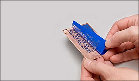
5. Masking and Resist
Masking and resist materials are used to protect the desired conductive traces from the etchant solution during the etching process. The most common masking and resist methods include:
- Photoresist: A light-sensitive material that is applied to the PCB surface and exposed to UV light through a photomask to create the desired etching pattern.
- Solder mask: A permanent protective coating that is applied to the PCB surface to protect the conductive traces and prevent solder bridging.
- Dry film resist: A pre-sensitized film that is laminated onto the PCB surface and exposed to UV light to create the etching pattern.
The choice of masking and resist material depends on factors such as the PCB design complexity, desired feature size, and production volume. Proper application and development of the masking and resist materials are crucial for achieving accurate and reliable etching results.

PCB Etching Process Steps
The PCB etching process typically involves the following steps:
- PCB Design and Artwork Preparation
- Create the PCB design using specialized software or tools.
- Generate the necessary artwork files, such as Gerber files or CAD drawings.
-
Ensure the artwork meets the manufacturing specifications and design rules.
-
PCB cleaning and Preparation
- Clean the PCB substrate to remove any contaminants or debris.
- Apply the masking or resist material to the PCB surface according to the chosen method.
- Expose the resist material to UV light through a photomask to create the desired etching pattern.
-
Develop the resist material to reveal the exposed copper areas.
-
Etching Process
- Prepare the etchant solution according to the manufacturer’s instructions.
- Immerse the PCB in the etchant solution and ensure proper agitation.
- Control the etching time and temperature based on the PCB material and desired etch depth.
-
Monitor the etching progress and remove the PCB from the etchant solution once the unwanted copper is completely removed.
-
Post-Etching Cleaning and Finishing
- Rinse the PCB thoroughly with water to remove any residual etchant solution.
- Remove the masking or resist material using an appropriate solvent or stripping process.
- Inspect the PCB for any defects or incomplete etching.
- Apply additional finishing processes, such as solder mask application or surface finish, if required.

Common PCB Etching Defects and Troubleshooting
Despite following the proper etching process, defects can sometimes occur. Here are some common PCB etching defects and their possible causes:
1. Over-Etching
- Cause: Excessive etching time or temperature
- Solution: Reduce the etching time or temperature and monitor the process closely
2. Under-Etching
- Cause: Insufficient etching time or weak etchant solution
- Solution: Increase the etching time or replenish the etchant solution
3. Etch Pits
- Cause: Uneven etching or contamination on the PCB surface
- Solution: Ensure proper cleaning of the PCB and maintain consistent agitation during etching
4. Broken or Incomplete Traces
- Cause: Insufficient masking or resist coverage, or damage during handling
- Solution: Improve the masking or resist application process and handle the PCB carefully
5. Rough or Uneven Edges
- Cause: Poor artwork quality or insufficient agitation during etching
- Solution: Use high-quality artwork files and ensure proper agitation throughout the etching process
Best Practices for Achieving Perfect PCB Etching
To achieve the perfect PCB etching results, consider the following best practices:
- Use high-quality PCB materials and etchant solutions from reputable suppliers.
- Ensure proper cleaning and preparation of the PCB surface before etching.
- Follow the manufacturer’s instructions for the etchant solution preparation and handling.
- Control the etching time and temperature precisely based on the PCB material and desired etch depth.
- Maintain consistent agitation during the etching process to ensure uniform etching.
- Use appropriate masking or resist materials and ensure proper application and development.
- Regularly inspect the etching progress and adjust the process parameters if necessary.
- Implement proper safety measures and dispose of the etchant solution according to local regulations.
- Conduct thorough post-etching cleaning and inspection to identify any defects or issues.
- Continuously monitor and optimize the etching process based on the results and feedback.
Frequently Asked Questions (FAQ)
- What is the most commonly used etchant solution for PCB etching?
-
Ferric Chloride (FeCl3) is the most widely used etchant solution for PCB etching due to its effectiveness and availability.
-
Can I reuse the etchant solution for multiple etching cycles?
-
While it is possible to reuse the etchant solution, its effectiveness may decrease over time. It is recommended to monitor the etchant solution’s performance and replenish or replace it as needed.
-
How do I dispose of the used etchant solution safely?
-
The used etchant solution should be neutralized and disposed of according to local environmental regulations. Consult with your local authorities or waste management service for proper disposal guidelines.
-
What is the best way to ensure uniform etching during the PCB etching process?
-
Proper agitation of the etchant solution is crucial for achieving uniform etching. This can be achieved through mechanical stirring, air bubbling, or ultrasonic agitation.
-
How can I prevent over-etching or under-etching during the PCB etching process?
- To prevent over-etching or under-etching, carefully control the etching time and temperature based on the PCB material and desired etch depth. Regularly monitor the etching progress and adjust the process parameters if necessary.
Conclusion
PCB etching is a critical process in the manufacturing of high-quality printed circuit boards. By understanding the different etching methods, factors affecting etching quality, and best practices, you can achieve the perfect PCB etching results.
Whether you opt for chemical etching, laser etching, or mechanical etching, it is essential to select the appropriate PCB materials, etchant solutions, and process parameters. Proper masking and resist application, precise control of etching time and temperature, and consistent agitation are key to obtaining clean and accurate etching results.
By following the guidelines outlined in this comprehensive guide and continuously optimizing your etching process, you can produce PCBs with excellent functionality, reliability, and appearance. Remember to prioritize safety, adhere to environmental regulations, and seek professional assistance when necessary.
With dedication and attention to detail, you can master the art of PCB etching and create perfect PCBs for your projects and applications.


Leave a Reply