What is Solder Mask?
Solder mask, also known as solder resist or solder stop, is a thin layer of polymer applied to the copper traces of a printed circuit board (PCB). Its primary purpose is to prevent solder from adhering to areas where it is not intended, thus protecting the circuit from short circuits and other potential issues during the soldering process. Solder mask also serves as an insulator, preventing electrical contact between adjacent traces and components.
Key Functions of Solder Mask
- Prevents solder bridging
- Insulates copper traces
- Protects PCB from environmental factors
- Improves PCB aesthetics
Types of Solder Mask
There are several types of solder mask available, each with its own unique properties and applications.
Liquid Photoimageable Solder Mask (LPISM)
LPISM is the most common type of solder mask used in PCB manufacturing. It is applied as a liquid and then exposed to UV light through a photographic film, which hardens the exposed areas. The unexposed areas are then washed away, leaving the desired solder mask pattern.
Dry Film Photoimageable Solder Mask (DFISM)
DFISM is similar to LPISM but is applied as a dry film instead of a liquid. The film is laminated onto the PCB surface, exposed to UV light, and then developed. This type of solder mask is often used for high-volume production due to its ease of application and consistency.
Liquid Photoimageable Solder Mask (LPISM) vs. Dry Film Photoimageable Solder Mask (DFISM)
| Property | LPISM | DFISM |
|---|---|---|
| Application Method | Liquid | Dry Film |
| Thickness Control | More Difficult | Easier |
| Resolution | Higher | Lower |
| Cost | Lower | Higher |
| Ease of Use | More Complex | Simpler |
Other Types of Solder Mask
- Screen Printed Solder Mask
- Peelable Solder Mask
- Thermal Cured Solder Mask

Solder Mask Application Process
The solder mask application process varies depending on the type of solder mask being used. However, the general steps are as follows:
-
PCB cleaning: The PCB surface is cleaned to remove any contaminants that may affect solder mask adhesion.
-
Solder Mask Application: The solder mask is applied to the PCB surface using the chosen method (e.g., screen printing, lamination, or spraying).
-
Exposure: The solder mask is exposed to UV light through a photographic film or direct imaging system, which hardens the exposed areas.
-
Development: The unexposed areas of the solder mask are washed away using a developer solution, leaving the desired solder mask pattern.
-
Curing: The solder mask is cured using heat to improve its mechanical and chemical properties.
-
Inspection: The PCB is inspected for any defects or imperfections in the solder mask.

Solder Mask Properties and Specifications
When selecting a solder mask for a specific application, several properties and specifications should be considered:
Electrical Properties
- Dielectric Strength
- Insulation Resistance
- Dielectric Constant
- Dissipation Factor
Mechanical Properties
- Adhesion
- Hardness
- Flexibility
- Abrasion Resistance
Chemical Properties
- Resistance to Solvents
- Resistance to Acids and Alkalines
- Flammability
Other Specifications
- Thickness
- Color
- Thermal Resistance
- UV Resistance

Solder Mask Colors and Finishes
Solder masks are available in a variety of colors and finishes to suit different applications and aesthetic preferences. The most common colors are green, blue, red, and black. Some specialized applications may require other colors, such as white or clear.
Solder mask finishes can be either glossy or matte, depending on the desired appearance and functionality. Glossy finishes are often used for high-end products, while matte finishes are more common in industrial applications.
Solder Mask Design Considerations
When designing a PCB with solder mask, several factors should be taken into account to ensure optimal performance and manufacturability:
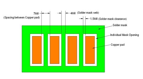
Clearance and Spacing
Proper clearance and spacing between components, pads, and traces are essential to prevent solder bridging and ensure adequate insulation. The solder mask should be designed with sufficient clearance around critical areas to accommodate manufacturing tolerances.
Solder Mask Expansion
During the curing process, solder mask may expand slightly. This expansion should be accounted for in the design to prevent encroachment on pads or traces.
Solder Mask Alignment
Proper alignment between the solder mask and the underlying copper features is crucial for ensuring reliable electrical connections. Misalignment can lead to exposed copper, solder bridging, or poor adhesion.
Solder Mask Thickness
The thickness of the solder mask can affect its insulation properties and the ease of soldering. Thicker solder masks provide better insulation but may make soldering more difficult. Thinner solder masks allow for easier soldering but may compromise insulation.
Solder Mask Defects and Troubleshooting
Several common defects can occur during the solder mask application process, which can affect the performance and reliability of the PCB:
Pinholes
Pinholes are small holes in the solder mask that expose the underlying copper. They can be caused by contaminants, air bubbles, or insufficient solder mask coverage. Pinholes can lead to solder bridging or corrosion.
Solder Mask Lifting
Solder mask lifting occurs when the solder mask separates from the PCB surface, exposing the copper beneath. This can be caused by poor adhesion, contamination, or excessive stress during the manufacturing process. Solder mask lifting can lead to electrical shorts or solder bridging.
Solder Mask Discoloration
Solder mask discoloration can occur due to exposure to high temperatures, UV light, or certain chemicals. While discoloration itself may not affect the performance of the PCB, it can be an indication of other issues, such as improper curing or contamination.
Troubleshooting Solder Mask Issues
- Ensure proper cleaning of the PCB surface before solder mask application.
- Verify that the solder mask is properly mixed and applied at the correct thickness.
- Check exposure and development settings to ensure complete curing and removal of unexposed areas.
- Inspect the PCB for any signs of contamination or damage.
- Adjust design parameters, such as clearance and spacing, to accommodate manufacturing tolerances.
Frequently Asked Questions (FAQ)
- What is the difference between solder mask and conformal coating?
-
Solder mask is applied before the soldering process to prevent solder from adhering to unintended areas, while conformal coating is applied after soldering to protect the PCB from environmental factors such as moisture, dust, and chemicals.
-
Can solder mask be removed?
-
Yes, solder mask can be removed using specialized chemicals or abrasive methods. However, removing solder mask can be difficult and may damage the underlying copper features if not done carefully.
-
How does solder mask affect the impedance of a PCB?
-
Solder mask can affect the impedance of a PCB by altering the dielectric constant of the surface. This effect is more pronounced at high frequencies and should be accounted for in the design of high-speed circuits.
-
What is the typical thickness of solder mask?
-
The typical thickness of solder mask ranges from 0.0005 to 0.002 inches (0.0127 to 0.0508 mm). The exact thickness depends on the specific application and the type of solder mask being used.
-
Can solder mask be applied to Flexible PCBs?
- Yes, solder mask can be applied to flexible PCBs. However, the choice of solder mask material and application process may differ from that used for rigid PCBs to accommodate the flexing and bending of the substrate.
Conclusion
Solder mask is an essential component of modern PCB manufacturing, providing insulation, protection, and improved aesthetics. Understanding the types, properties, and application processes of solder mask is crucial for designing and manufacturing reliable, high-quality PCBs. By considering factors such as clearance, spacing, expansion, alignment, and thickness, designers can ensure that their PCBs perform optimally and are protected from potential issues such as solder bridging and corrosion.
As PCB technology continues to advance, so too will the materials and techniques used in solder mask application. Staying up-to-date with the latest developments in solder mask technology will help designers and manufacturers create PCBs that meet the ever-increasing demands of modern electronics.


Leave a Reply