Introduction to PCB Layout and Differential Traces
Printed Circuit Board (PCB) layout is a crucial aspect of electronic design, as it determines the performance, reliability, and manufacturability of the final product. One of the key challenges in PCB layout is ensuring the proper alignment and routing of differential traces and serpentine lines. In this article, we will delve into the best practices and techniques for achieving right angle alignment of differential traces and serpentine lines in PCB layout.
What are Differential Traces?
Differential traces are pairs of interconnects that carry differential signals, which are two complementary signals that are equal in magnitude but opposite in polarity. Differential signaling is widely used in high-speed digital communication systems, such as USB, HDMI, and PCIe, due to its superior noise immunity and signal integrity compared to single-ended signaling.
The Importance of Right Angle Alignment
Proper alignment of differential traces is essential to maintain the signal integrity and minimize crosstalk between the traces. When differential traces are not aligned properly, the signals can become unbalanced, leading to common mode noise and signal degradation. Right angle alignment, where the traces are perpendicular to each other, is considered the best practice for differential trace routing.
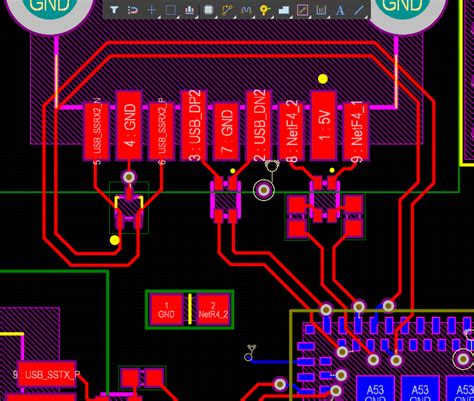
Techniques for Right Angle Alignment of Differential Traces
1. Trace Width and Spacing
The first step in achieving right angle alignment is to determine the appropriate trace width and spacing for the differential traces. The trace width should be chosen based on the required impedance and current carrying capacity, while the spacing between the traces should be optimized to minimize crosstalk and maintain signal integrity.
The following table provides general guidelines for trace width and spacing based on the desired impedance:
| Impedance (Ω) | Trace Width (mil) | Trace Spacing (mil) |
|---|---|---|
| 50 | 10 | 6 |
| 75 | 8 | 8 |
| 100 | 6 | 10 |
2. Serpentine Routing
Serpentine routing is a technique used to match the lengths of differential traces by adding gentle curves or zigzags to the shorter trace. This is necessary because any mismatch in the lengths of the differential traces can lead to signal skew and degradation.
When implementing serpentine routing, it is important to follow these guidelines:
- Keep the curves smooth and gradual to minimize discontinuities and reflections.
- Maintain a consistent spacing between the traces throughout the serpentine section.
- Avoid sharp corners or abrupt changes in direction, as they can cause impedance mismatch and signal integrity issues.
3. Via Placement and Routing
Vias are used to transition between layers in a Multi-Layer PCB. When routing differential traces, it is crucial to place the vias in a way that maintains the right angle alignment and minimizes the via stub length.
Consider the following best practices for via placement and routing:
- Place the vias for the differential traces as close together as possible to minimize the via-to-via spacing.
- Route the traces to the vias at a right angle to maintain the perpendicular alignment.
- Keep the via stub length as short as possible to reduce the capacitance and inductance associated with the via.
4. Layer Transitions
When differential traces transition between layers, it is essential to maintain the right angle alignment and minimize the impedance discontinuity. One common technique is to use a technique called “stitching” or “staggering” of vias.
Stitching involves placing the vias for the differential traces on adjacent layers, with a small offset between them. This helps to maintain the right angle alignment and reduces the impedance discontinuity caused by the layer transition.

Serpentine Lines in PCB Layout
Serpentine lines are not only used for matching the lengths of differential traces but also for other purposes in PCB layout, such as:
- Delay matching: Serpentine lines can be used to introduce a specific amount of delay in a signal path to synchronize it with other signals.
- Impedance matching: By adjusting the width and spacing of the serpentine lines, the impedance of the trace can be fine-tuned to match the desired value.
- Crosstalk reduction: Serpentine lines can be used to increase the spacing between adjacent traces, thereby reducing the crosstalk between them.
Designing Serpentine Lines
When designing serpentine lines, it is important to consider the following factors:
- Line width: The width of the serpentine lines should be chosen based on the desired impedance and current carrying capacity.
- Line spacing: The spacing between the serpentine lines should be optimized to minimize crosstalk and maintain signal integrity.
- Number of turns: The number of turns in the serpentine line determines the amount of delay or impedance matching achieved. However, increasing the number of turns also increases the overall trace length and can impact the signal integrity.
The following table provides an example of how the number of turns in a serpentine line affects the delay and impedance:
| Number of Turns | Delay (ps) | Impedance (Ω) |
|---|---|---|
| 1 | 10 | 50 |
| 2 | 20 | 52 |
| 3 | 30 | 55 |
| 4 | 40 | 58 |

Simulation and Verification
Once the PCB layout is complete, it is essential to simulate and verify the design to ensure that it meets the desired performance and signal integrity requirements. Several simulation tools are available, such as:
- SPICE-based simulators: These tools can simulate the electrical behavior of the PCB, including the differential traces and serpentine lines, and help identify any signal integrity issues.
- Electromagnetic (EM) simulators: EM simulators can provide a more accurate analysis of the PCB layout by taking into account the physical properties of the materials and the coupling between traces.
- Time-domain reflectometry (TDR) analysis: TDR analysis can help identify impedance discontinuities and signal reflections in the PCB layout.
By simulating and verifying the PCB layout, designers can identify and address any issues before the board is manufactured, saving time and cost in the long run.

Conclusion
Right angle alignment of differential traces and serpentine lines is crucial for maintaining signal integrity and performance in PCB layout. By following best practices such as optimizing trace width and spacing, implementing serpentine routing, proper via placement, and using layer transition techniques like stitching, designers can achieve a robust and reliable PCB Design.
Additionally, the use of serpentine lines for delay matching, impedance matching, and crosstalk reduction can further enhance the performance of the PCB. Simulation and verification tools play a vital role in validating the design and identifying any potential issues before manufacturing.
By understanding and applying these techniques, PCB designers can create high-quality layouts that meet the demanding requirements of modern electronic systems.
Frequently Asked Questions (FAQ)
-
Q: What is the purpose of right angle alignment in differential traces?
A: Right angle alignment helps maintain signal integrity and minimize crosstalk between differential traces by ensuring that the traces are perpendicular to each other. -
Q: How does serpentine routing help in differential trace routing?
A: Serpentine routing is used to match the lengths of differential traces by adding gentle curves or zigzags to the shorter trace, thereby minimizing signal skew and degradation. -
Q: What are the key factors to consider when designing serpentine lines?
A: When designing serpentine lines, the key factors to consider are line width, line spacing, and the number of turns. These factors affect the impedance, delay, and signal integrity of the traces. -
Q: Why is via placement important in differential trace routing?
A: Proper via placement is crucial to maintain the right angle alignment and minimize the via stub length, which helps reduce the capacitance and inductance associated with the via. -
Q: What are the benefits of simulating and verifying the PCB layout?
A: Simulating and verifying the PCB layout helps identify and address any signal integrity issues before the board is manufactured, saving time and cost in the long run. It ensures that the design meets the desired performance and reliability requirements.


Leave a Reply