Introduction to KiCad and PCB Design
KiCad is a free and open-source electronic design automation (EDA) software that enables users to design printed circuit boards (PCBs). It provides a complete set of tools for schematic capture, PCB layout, and gerber file generation. In this comprehensive guide, we will walk you through the process of creating a PCB using KiCad, from setting up the software to generating the final manufacturing files.
What is a PCB?
A printed circuit board (PCB) is a flat board made of insulating material, such as fiberglass or plastic, with conductive copper traces printed on its surface. These traces connect various electronic components, such as resistors, capacitors, and integrated circuits (ICs), to form a functional electronic circuit. PCBs are used in almost all electronic devices, from simple gadgets to complex industrial equipment.
Why Use KiCad for PCB Design?
KiCad offers several advantages over other EDA software:
- Free and open-source: KiCad is available at no cost and is supported by a large community of developers and users.
- Cross-platform compatibility: KiCad runs on Windows, macOS, and Linux, making it accessible to a wide range of users.
- Extensive component libraries: KiCad comes with a vast collection of component libraries, and users can also create custom libraries.
- Powerful design tools: KiCad provides a comprehensive set of tools for schematic capture, PCB layout, and design rule checking (DRC).
- Active community support: The KiCad community is active and helpful, providing resources, tutorials, and forums for users to learn and troubleshoot issues.
Setting Up KiCad
Before we begin designing our PCB, let’s set up KiCad on our computer.
Downloading and Installing KiCad
- Visit the official KiCad website: https://www.kicad.org/
- Click on the “Download” button and select the appropriate version for your operating system.
- Follow the installation instructions for your operating system.
Configuring KiCad
After installing KiCad, you may need to configure some settings to suit your preferences and work environment.
- Launch KiCad and click on “Preferences” in the top menu.
- In the “Preferences” window, you can customize various settings, such as the default units (mm or inches), canvas colors, and hotkey assignments.
- Click “OK” to save your settings.

Creating a New Project
To start designing our PCB, we need to create a new project in KiCad.
- In the KiCad main window, click on “File” > “New Project.”
- Choose a location to save your project and give it a name.
- Click “Save” to create the project.

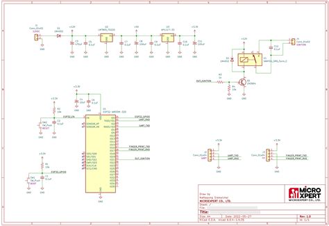
Designing the Schematic
The first step in creating a PCB is to design the schematic, which represents the electrical connections between components.
Creating a New Schematic
- In the KiCad project window, double-click on the “Schematic Layout Editor” icon.
- Click on “File” > “New Schematic.”
- Save the schematic with a descriptive name, such as “main_schematic.”
Adding Components
To add components to your schematic:
- Click on the “Place symbol” button in the toolbar or press the “A” key.
- In the component library browser, search for the desired component and double-click on it to add it to the schematic.
- Place the component on the schematic canvas by clicking on the desired location.
- Repeat steps 1-3 for all the components in your circuit.
Connecting Components with Wires
To connect components using wires:
- Click on the “Place wire” button in the toolbar or press the “W” key.
- Click on the first component pin you want to connect.
- Move the cursor to the second component pin and click to complete the connection.
- Repeat steps 1-3 for all the necessary connections in your circuit.
Labeling Wires and Components
To make your schematic more readable and easier to understand, label your wires and components:
- Click on the “Place net name” button in the toolbar or press the “L” key.
- Click on the wire you want to label and type the desired name.
- To label components, click on the “Place text” button in the toolbar or press the “T” key, then click on the component and type the desired label.
Running Electrical Rules Check (ERC)
Before proceeding to PCB layout, it’s essential to run an Electrical Rules Check (ERC) to ensure that your schematic is free of errors.
- Click on “Inspect” > “Electrical Rules Check” in the top menu.
- In the ERC window, click on “Run.”
- If any errors or warnings are detected, address them before moving on to PCB layout.

PCB Layout
Once your schematic is complete and error-free, you can begin the PCB layout process.
Generating a Netlist
A netlist is a file that contains information about the connections between components in your schematic. To generate a netlist:
- In the schematic editor, click on “Tools” > “Generate Netlist File.”
- Save the netlist file in your project directory.
Creating a New PCB Layout
- In the KiCad project window, double-click on the “PCB Layout Editor” icon.
- Click on “File” > “New Board.”
- Save the PCB layout with a descriptive name, such as “main_pcb.”
Importing the Netlist
To transfer the component connections from your schematic to the PCB layout:
- In the PCB layout editor, click on “Tools” > “Update PCB from Schematic.”
- Select the netlist file you generated earlier and click “Open.”
- The components from your schematic will now appear in the PCB layout editor.
Placing Components
Arrange the components on the PCB layout canvas:
- Click and drag the components to their desired positions.
- Use the “Move” tool (M) and the “Rotate” tool (R) to fine-tune the component placement.
- Ensure that components are placed logically and with sufficient space between them for routing traces.
Routing Traces
To connect the components on the PCB:
- Click on the “Route Tracks” button in the toolbar or press the “X” key.
- Click on the first component pad you want to connect.
- Move the cursor to the second component pad and click to complete the connection.
- Repeat steps 1-3 for all the necessary connections on your PCB.
- Use the “Add Via” tool to create vias (connections between layers) when necessary.
Running Design Rule Check (DRC)
Before finalizing your PCB layout, run a Design Rule Check (DRC) to ensure that your design meets the manufacturing requirements:
- Click on “Inspect” > “Design Rules Checker” in the top menu.
- Configure the DRC settings according to your PCB manufacturer’s specifications.
- Click on “Run DRC.”
- If any errors or warnings are detected, address them before proceeding.
Generating Manufacturing Files
Once your PCB layout is complete and has passed the DRC, you can generate the files needed for manufacturing.
Generating Gerber Files
Gerber files are the standard format used by PCB manufacturers. To generate Gerber files:
- In the PCB layout editor, click on “File” > “Plot.”
- In the “Plot” window, select the layers you want to include in the Gerber files (e.g., copper layers, solder mask, and silkscreen).
- Set the output directory and click “Plot” to generate the Gerber files.
Generating Drill Files
Drill files contain information about the holes and vias on your PCB. To generate drill files:
- In the PCB layout editor, click on “File” > “Fabrication Outputs” > “Drill Files.”
- Set the output directory and click “Generate Drill File.”
Exporting the Bill of Materials (BOM)
The Bill of Materials (BOM) is a list of all the components used in your PCB. To export the BOM:
- In the schematic editor, click on “Tools” > “Generate Bill of Materials.”
- Set the output file format and location, then click “Generate.”
Sending Files to a PCB Manufacturer
With your manufacturing files generated, you can now send them to a PCB manufacturer for production.
- Research and select a reputable PCB manufacturer that meets your requirements (e.g., cost, turnaround time, and quality).
- Package your Gerber files, drill files, and BOM into a single compressed file (e.g., ZIP or RAR).
- Upload the compressed file to the manufacturer’s website or send it via email, following their specific instructions.
- Review and approve the manufacturer’s design files and production details before confirming your order.
Frequently Asked Questions (FAQ)
-
Q: Can I design a multi-layer PCB using KiCad?
A: Yes, KiCad supports the design of multi-layer PCBs. You can specify the number of layers and their properties in the PCB layout editor. -
Q: How do I create custom footprints for components not found in the KiCad libraries?
A: You can create custom footprints using the Footprint Editor in KiCad. This tool allows you to design and save custom footprints for use in your PCB layouts. -
Q: Can I import designs from other EDA software into KiCad?
A: Yes, KiCad supports importing designs from other EDA software, such as Eagle and Altium Designer. You can use the “Import” function in the schematic and PCB layout editors to bring in external files. -
Q: How do I create a ground plane in KiCad?
A: To create a ground plane in KiCad, use the “Add Filled Zone” tool in the PCB layout editor. Set the zone properties to “GND” (or your desired net name) and configure the fill settings. -
Q: What should I do if I encounter issues or have questions while using KiCad?
A: The KiCad community is an excellent resource for troubleshooting and learning. You can find help in the official KiCad forums, online tutorials, and user groups. Additionally, the official KiCad documentation provides detailed information on the software’s features and tools.
Conclusion
Designing a PCB using KiCad is a straightforward process that can be mastered with practice and attention to detail. By following this guide, you should now have a solid understanding of the steps involved in creating a PCB, from setting up the software to generating manufacturing files. Remember to always double-check your designs, run ERC and DRC checks, and carefully review your files before sending them to a manufacturer. With KiCad’s powerful tools and the support of its community, you’ll be well on your way to creating professional-quality PCBs for your projects.


Leave a Reply