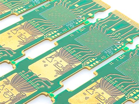
What is Electroplated Nickel PCB?
Electroplated nickel PCB refers to a printed circuit board that has undergone the electroplating process to deposit a layer of nickel onto its surface. The nickel layer is typically applied over the copper traces and pads of the PCB to enhance its properties, such as solderability, wear resistance, and electrical conductivity.
The electroplated nickel layer on a PCB serves several purposes:
-
Solderability: Nickel provides an excellent surface for soldering components onto the PCB. It prevents the oxidation of the copper surface, which can hinder the soldering process.
-
Corrosion resistance: Nickel is resistant to corrosion, protecting the underlying copper from environmental factors that can degrade its performance over time.
-
Wear resistance: The nickel layer offers increased wear resistance, making the PCB more durable and extending its lifespan.
-
Electrical conductivity: Nickel is an excellent conductor of electricity, ensuring efficient signal transmission throughout the PCB.
The Electroplated Nickel PCB Process
The electroplated nickel PCB process involves several steps to achieve a uniform and high-quality nickel finish on the printed circuit board. Here is an overview of the process:
Step 1: Surface Preparation
Before the electroplating process can begin, the PCB surface must be thoroughly cleaned and prepared. This step involves removing any contaminants, such as dirt, grease, or oxides, from the copper surface. The PCB is typically cleaned using a combination of chemical and mechanical methods, such as:
- Alkaline cleaning: The PCB is immersed in an alkaline solution to remove organic contaminants and oils.
- Micro-etching: A mild etching solution is used to remove any remaining oxides and provide a slightly roughened surface for better adhesion of the nickel layer.
- Acid dipping: The PCB is dipped in an acidic solution to remove any residual contaminants and activate the copper surface.
Step 2: Electroplating Bath Preparation
The electroplating bath is a critical component of the electroplated nickel PCB process. The bath contains a solution of nickel salts, such as nickel sulfate or nickel chloride, along with various additives that help control the properties of the deposited nickel layer.
The composition of the electroplating bath can vary depending on the specific requirements of the PCB, such as the desired thickness, brightness, and internal stress of the nickel layer. The bath is maintained at a specific temperature and pH level to ensure optimal plating conditions.
Step 3: Electroplating Process
Once the PCB surface is prepared and the electroplating bath is ready, the actual electroplating process can begin. The PCB is immersed in the electroplating bath, and an electric current is applied between the PCB (cathode) and a nickel anode.
As the electric current flows through the solution, nickel ions are reduced at the cathode (PCB surface), forming a thin layer of nickel metal. The thickness of the nickel layer can be controlled by adjusting the current density and the duration of the electroplating process.
Typical nickel layer thicknesses for PCBs range from 1 to 5 microns, depending on the specific application requirements.
Step 4: Post-Plating Treatment
After the electroplating process is complete, the PCB undergoes several post-plating treatments to enhance the properties of the nickel layer and prepare it for subsequent processing steps.
-
Rinsing: The PCB is rinsed with deionized water to remove any residual plating solution and prevent contamination of subsequent processes.
-
Drying: The PCB is dried using hot air or an oven to remove any moisture from the surface.
-
Annealing: In some cases, the PCB may undergo an annealing process to relieve internal stresses in the nickel layer and improve its mechanical properties.
-
Inspection: The PCB is inspected for any defects, such as pinholes, blisters, or uneven plating. Various techniques, such as visual inspection, cross-sectional analysis, and thickness measurements, may be employed to ensure the quality of the electroplated nickel layer.

Advantages of Electroplated Nickel PCB
Electroplated nickel PCBs offer several advantages over other surface finishes:
-
Excellent solderability: The nickel layer provides a uniform and oxide-free surface that promotes good wetting and strong solder joint formation.
-
Enhanced corrosion resistance: Nickel is resistant to corrosion, protecting the underlying copper from environmental factors that can degrade its performance.
-
Improved wear resistance: The hardness of the nickel layer offers increased wear resistance, making the PCB more durable and extending its lifespan.
-
Good electrical conductivity: Nickel is an excellent conductor of electricity, ensuring efficient signal transmission throughout the PCB.
-
Cost-effective: Electroplated nickel is a relatively cost-effective surface finish compared to other options, such as gold or silver.
-
Compatibility with various soldering processes: Electroplated nickel is compatible with a wide range of soldering processes, including reflow soldering, wave soldering, and hand soldering.

Applications of Electroplated Nickel PCB
Electroplated nickel PCBs find applications in various industries and products:
-
Consumer electronics: Electroplated nickel is commonly used in consumer electronic devices, such as smartphones, tablets, and laptops, where good solderability and corrosion resistance are essential.
-
Automotive electronics: The automotive industry relies on electroplated nickel PCBs for their durability and resistance to harsh environmental conditions.
-
Industrial equipment: Electroplated nickel PCBs are used in industrial equipment, such as control systems and automation devices, where reliability and long-term performance are critical.
-
Medical devices: The biocompatibility and corrosion resistance of electroplated nickel make it suitable for use in medical devices and equipment.
-
Aerospace and defense: Electroplated nickel PCBs are used in aerospace and defense applications, where high reliability and resistance to extreme conditions are paramount.

Frequently Asked Questions (FAQ)
- What is the typical thickness of the electroplated nickel layer on a PCB?
The typical thickness of the electroplated nickel layer on a PCB ranges from 1 to 5 microns, depending on the specific application requirements.
- Can electroplated nickel be used for both through-hole and surface-mount components?
Yes, electroplated nickel is suitable for both through-hole and surface-mount components. The nickel layer provides a uniform surface for soldering, ensuring good solder joint formation.
- How does electroplated nickel compare to other surface finishes, such as ENIG or immersion silver?
Electroplated nickel offers several advantages over other surface finishes, such as its cost-effectiveness, excellent solderability, and good wear resistance. However, other finishes like ENIG (Electroless Nickel Immersion Gold) or immersion silver may be preferred for specific applications due to their unique properties, such as better corrosion resistance or compatibility with wire bonding.
- Is electroplated nickel suitable for high-frequency PCB applications?
Electroplated nickel is generally suitable for high-frequency PCB applications due to its good electrical conductivity. However, in some cases, other surface finishes like immersion silver or gold may be preferred for their superior high-frequency performance.
- How does the electroplating process affect the dimensions of the PCB features?
The electroplating process can slightly increase the dimensions of the PCB features, such as the thickness of the copper traces and the diameter of the holes. This dimensional change should be accounted for during the PCB design phase to ensure that the final product meets the required specifications.
Conclusion
Electroplated nickel is a widely used surface finish for printed circuit boards, offering excellent solderability, corrosion resistance, and wear resistance. The electroplated nickel PCB process involves a series of steps, including surface preparation, electroplating bath preparation, the actual electroplating process, and post-plating treatments.
Electroplated nickel PCBs find applications in various industries, such as consumer electronics, automotive electronics, industrial equipment, medical devices, and aerospace and defense. The choice of electroplated nickel over other surface finishes depends on the specific requirements of the application, such as cost, performance, and compatibility with subsequent manufacturing processes.
By understanding the electroplated nickel PCB process, its advantages, and its applications, PCB designers and manufacturers can make informed decisions when selecting the most suitable surface finish for their products.


Leave a Reply