What is ENIG-BP?
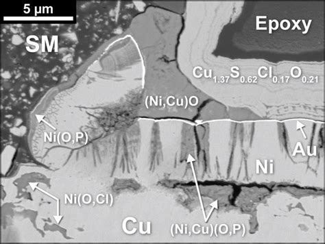
ENIG-Black Pad (ENIG-BP) is a defect that can occur in printed circuit boards (PCBs) when using the Electroless Nickel Immersion Gold (ENIG) surface finish. This issue is characterized by the formation of a black or dark brown discoloration on the nickel surface beneath the gold layer, which can lead to poor solderability, reduced reliability, and potential failure of the PCB assembly.
Causes of ENIG-BP
Several factors can contribute to the development of ENIG-Black Pad:
-
Excessive nickel corrosion: If the nickel layer is exposed to the immersion gold bath for too long, it can result in excessive corrosion of the nickel surface, leading to the formation of a black pad.
-
Inadequate gold thickness: A thin or uneven gold layer may not provide sufficient protection for the underlying nickel, allowing it to corrode and form a black pad.
-
Contamination: Impurities in the ENIG process baths, such as organic contaminants or heavy metals, can accelerate the corrosion of the nickel layer and promote the formation of black pads.
-
Improper process control: Deviations from the optimal process parameters, such as temperature, pH, or concentration of the plating baths, can lead to the development of ENIG-BP.
Impact of ENIG-BP on PCB Assembly
ENIG-Black Pad can have several negative effects on the PCB assembly process and the final product:
-
Poor solderability: The black or dark brown discoloration on the nickel surface can hinder the wetting of the solder, resulting in weak or incomplete solder joints.
-
Reduced reliability: Weak solder joints caused by ENIG-BP can lead to premature failure of the PCB assembly, especially under stress conditions such as thermal cycling or vibration.
-
Increased rework and scrap: PCBs affected by ENIG-BP may require rework or may need to be scrapped, resulting in increased production costs and delays.
Mitigating ENIG-BP
To minimize the occurrence of ENIG-Black Pad, several strategies can be implemented:
Process Optimization
Optimizing the ENIG process parameters is crucial for reducing the risk of ENIG-BP. This includes:
-
Controlling the immersion gold bath: Ensure that the gold bath concentration, temperature, and immersion time are within the recommended ranges to avoid excessive nickel corrosion.
-
Maintaining proper nickel thickness: A sufficiently thick nickel layer (typically 3-6 μm) can help prevent the formation of black pads by providing a more robust barrier against corrosion.
-
Minimizing contamination: Regularly monitor and maintain the purity of the ENIG process baths to prevent the build-up of contaminants that can promote black pad formation.
Alternative Surface Finishes
In some cases, it may be necessary to consider alternative surface finishes to ENIG, especially for high-reliability applications. Some options include:
-
Immersion Silver (IAg): IAg provides good solderability and is less prone to black pad formation compared to ENIG.
-
Organic Solderability Preservative (OSP): OSP is a cost-effective alternative that offers good solderability and eliminates the risk of black pad formation associated with ENIG.
-
Electroless Palladium Immersion Gold (EPIG): EPIG is a more expensive option but offers excellent solderability and resistance to black pad formation.
Design Considerations
PCB designers can also take steps to minimize the impact of ENIG-BP:
-
Pad size and shape: Using larger, rounder pads can help improve solder joint strength and reduce the impact of black pads on solderability.
-
Solder mask design: Ensuring a proper solder mask opening around the pads can help promote better solder wetting and minimize the effect of black pads.
-
Component selection: Choosing components with more forgiving lead designs, such as gull-wing or J-lead, can help compensate for the reduced solderability caused by ENIG-BP.
Detecting and Addressing ENIG-BP
Visual Inspection
ENIG-Black Pad can often be detected through visual inspection of the PCB surface. The affected pads will appear black or dark brown, in contrast to the normal gold color of the ENIG finish. However, it is important to note that not all instances of ENIG-BP are visible to the naked eye, and more advanced detection methods may be necessary.
Solderability Testing
Solderability testing is a crucial step in identifying and assessing the impact of ENIG-BP on PCB assembly. Some common solderability tests include:
-
Wetting Balance Test: This test measures the wetting force and time of a solder ball on the PCB pad surface, providing a quantitative assessment of solderability.
-
Dip and Look Test: In this test, the PCB is dipped into a solder bath and then visually inspected for the presence of non-wetted or poorly wetted areas, which may indicate the presence of ENIG-BP.
-
Spread Test: A small amount of solder paste is placed on the PCB pad and reflowed, and the resulting solder spread is measured to assess solderability.
Addressing Affected PCBs
If ENIG-BP is detected on a PCB, there are several options for addressing the issue:
-
Rework: In some cases, affected pads can be reworked by removing the black pad material and re-applying the ENIG finish. However, this process can be time-consuming and may not be feasible for large-scale production.
-
Solder Pretreatment: Applying a solder pretreatment, such as a flux or a reducing agent, to the affected pads can help improve solderability and mitigate the impact of ENIG-BP.
-
Scrap and Replace: If the extent of ENIG-BP is severe or if rework is not possible, it may be necessary to scrap the affected PCBs and replace them with new ones.

FAQ
-
Q: What is the main cause of ENIG-Black Pad?
A: The main cause of ENIG-Black Pad is excessive corrosion of the nickel layer beneath the immersion gold surface finish. This can be due to factors such as prolonged exposure to the gold bath, insufficient gold thickness, contamination, or improper process control. -
Q: How does ENIG-BP affect PCB assembly?
A: ENIG-Black Pad can lead to poor solderability, resulting in weak or incomplete solder joints. This can reduce the reliability of the PCB assembly and increase the risk of premature failure, especially under stress conditions. PCBs affected by ENIG-BP may require rework or may need to be scrapped, leading to increased production costs and delays. -
Q: What are some strategies for mitigating ENIG-BP?
A: Strategies for mitigating ENIG-BP include optimizing the ENIG process parameters (such as controlling the gold bath, maintaining proper nickel thickness, and minimizing contamination), considering alternative surface finishes (such as Immersion Silver, OSP, or EPIG), and implementing design considerations (such as using larger, rounder pads and ensuring proper solder mask opening). -
Q: How can ENIG-BP be detected?
A: ENIG-Black Pad can often be detected through visual inspection of the PCB surface, as the affected pads will appear black or dark brown. Solderability testing, such as the Wetting Balance Test, Dip and Look Test, or Spread Test, can also be used to identify and assess the impact of ENIG-BP on PCB assembly. -
Q: What should be done if ENIG-BP is detected on a PCB?
A: If ENIG-BP is detected on a PCB, options for addressing the issue include reworking the affected pads by removing the black pad material and re-applying the ENIG finish, applying a solder pretreatment (such as a flux or reducing agent) to improve solderability, or scrapping and replacing the affected PCBs if the extent of ENIG-BP is severe or if rework is not possible.
| Factor | Contribution to ENIG-BP |
|---|---|
| Excessive nickel corrosion | Prolonged exposure to the immersion gold bath can lead to excessive nickel corrosion |
| Inadequate gold thickness | A thin or uneven gold layer may not provide sufficient protection for the nickel |
| Contamination | Impurities in the ENIG process baths can accelerate nickel corrosion |
| Improper process control | Deviations from optimal process parameters can promote ENIG-BP formation |
| Strategy | Description |
|---|---|
| Process Optimization | Optimize ENIG process parameters (gold bath control, nickel thickness, minimizing contamination) |
| Alternative Surface Finishes | Consider alternatives such as Immersion Silver, OSP, or EPIG |
| Design Considerations | Use larger, rounder pads; ensure proper solder mask opening; choose forgiving component leads |
| Detection Method | Description |
|---|---|
| Visual Inspection | Inspect PCB surface for black or dark brown pads |
| Wetting Balance Test | Measure wetting force and time of solder ball on pad surface |
| Dip and Look Test | Dip PCB in solder bath and visually inspect for non-wetted or poorly wetted areas |
| Spread Test | Place solder paste on pad, reflow, and measure resulting solder spread |
In conclusion, ENIG-Black Pad is a critical issue that can significantly impact the quality and reliability of PCB assemblies. By understanding the causes, effects, and mitigation strategies for ENIG-BP, PCB manufacturers and assemblers can take proactive steps to minimize its occurrence and ensure the production of high-quality, reliable electronic products. Regular monitoring, process optimization, and the consideration of alternative surface finishes and design practices can all contribute to reducing the risk of ENIG-BP and its associated costs and delays.
Leave a Reply