What is a PCB?
A printed circuit board (PCB) is the foundation of nearly all modern electronic devices. PCBs are flat boards made of insulating materials like fiberglass, with conductive copper traces printed on the surface. Electronic components like microchips, resistors, and capacitors are soldered onto the PCB to create a complete circuit.
PCBs provide several advantages over point-to-point wiring:
- Compact size
- Reduced electronic noise
- Easier to mass produce
- Lower manufacturing costs
PCB Manufacturing Process Overview
The PCB manufacturing process involves several key steps:
- PCB Design – Create the schematic and board layout using EDA software
- Film Generation – Print the PCB artwork onto plastic film
- Etching – Transfer the artwork to copper-clad board and etch away unwanted copper
- Drilling – Drill holes for through-hole components and vias
- Solder Mask Application – Add solder mask to insulate the copper traces
- Silkscreen – Print component labels and identifiers on the board
- Surface Finish – Apply surface finish to prevent copper oxidation
- Fabrication – Cut the panel into individual boards
- Electrical Testing – Test for shorts, opens and other manufacturing defects
- Component Assembly – Solder components onto the finished PCB

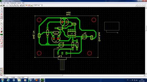
PCB Design
The first step in manufacturing a PCB is to design the circuit and create the board layout using EDA (electronic design automation) software. Popular EDA packages include:
- KiCad
- Eagle
- Altium Designer
- OrCAD
- Cadence Allegro
The PCB design process involves two main phases:
- Schematic capture – Draw the circuit diagram and specify components
- Board layout – Arrange components and route copper traces on the board
Key considerations during PCB design include:
- Selecting the appropriate board size and shape
- Choosing the number of layers (e.g. 2-layer vs 4-layer)
- Placing components to minimize trace lengths and avoid interference
- Ensuring adequate trace width for current carrying capacity
- Providing proper grounding and power distribution
- Adhering to RF and EMI best practices if applicable
- Complying with manufacturing design rules and tolerances

Film Generation
Once the PCB design is finalized, the next step is to generate the artwork films. The artwork contains the etching patterns for each layer of the board (copper, solder mask, silkscreen).
In the past, artworks were hand-taped using black crepe tape and clear mylar film. Today, artworks are generated digitally using a photoplotter or laser printer onto plastic film.
The printed films are usually black and clear, where black represents the areas to be etched away. The typical film dimensions are:
| Film Type | Imperial (in) | Metric (mm) |
|---|---|---|
| Copper | 16×20, 18×24, 21×24 | 406×508, 457×610, 533×610 |
| Solder Mask | 16×20, 18×24, 21×24 | 406×508, 457×610, 533×610 |
| Silkscreen | 16×20, 18×24, 21×24 | 406×508, 457×610, 533×610 |
It’s important to print the artworks at the correct scale factor, typically 1:1. The films should also be aligned precisely when taped together to form the panel.

Etching
With the artwork films ready, the next step is to transfer the etching pattern to the copper-clad board and remove the unwanted copper.
The copper-clad board consists of an insulating substrate material (usually FR-4 fiberglass) with thin copper foil laminated to one or both sides. The copper thickness is specified in ounces per square foot:
| Copper Weight (oz) | Thickness (mils) | Thickness (microns) |
|---|---|---|
| 0.5 | 0.7 | 17.5 |
| 1 | 1.4 | 35 |
| 2 | 2.8 | 70 |
The etching process involves several sub-steps:
- Scrubbing – Clean and roughen the copper surfaces
- Photoresist application – Laminate or coat the board with UV-sensitive film or liquid
- Exposure – Expose the photoresist to UV light through the artwork film
- Developing – Dissolve the unexposed photoresist in a chemical developer
- Etching – Spray or immerse the board in an acidic etchant solution to remove copper
- Stripping – Remove the remaining photoresist with a chemical stripper
Two common etching methods are:
- Acid etching – uses an acidic solution of ferric chloride, ammonium persulfate or cupric chloride
- Alkaline etching – uses an alkaline solution of ammoniacal copper chloride or sodium carbonate
After etching, the board is rinsed and inspected for defects like over/under-etching, shorts, opens, or hairline cracks.
Drilling
Most PCBs require holes to be drilled for mounting through-hole components or to create vias (connections between layers). Holes are drilled using high-speed CNC drilling machines with carbide drill bits.
Common hole sizes range from 0.2mm to 6mm in diameter. The hole size and location must match the component lead spacing within the specified tolerances.
The drilling process generates fiberglass dust, so proper vacuum collection and filtering is necessary. After drilling, the holes are cleaned of debris and inspected for burrs or cracks.
Solder Mask Application
The solder mask is an insulating layer that covers the copper traces on the PCB, except for the solder pads where components will be attached. The solder mask has several important functions:
- Prevents solder bridges from forming between traces
- Protects against oxidation and contamination
- Provides electrical insulation between conductors
- Improves appearance and readability
Solder mask is typically applied as a liquid photoimageable ink or dry film. The most common colors are green and blue, but other colors like red, yellow, black and white are available for specialized applications.
The solder mask application process is similar to etching:
- Solder mask application – Coat the board by screen printing (liquid) or vacuum lamination (dry film)
- Exposure – Expose the solder mask to UV light through a film artwork
- Developing – Dissolve the unexposed solder mask in a chemical developer
- Curing – Harden the solder mask by baking in an oven
After curing, the solder mask should be smooth, durable and well-adhered to the board. Solder mask height is typically 0.5-1.0 mils (12.7-25.4 microns) above the copper surface.
Silkscreen
The silkscreen layer contains the component identifiers, reference designators, logos and other markings on the PCB. Silkscreen is applied by screen printing a thermoset epoxy ink onto the solder mask.
Common silkscreen colors are white, black and yellow, depending on the solder mask color. The silkscreen ink must be compatible with the solder mask to ensure good adhesion.
The silkscreen artwork should follow good design practices for legibility:
- Minimum line width of 0.15mm (6 mils)
- Minimum text size of 1.5mm (60 mils)
- Use simple, sans-serif fonts
- Avoid placing text on pads or vias
- Provide adequate clearance around holes and board edges
After printing, the silkscreen is cured by baking in an oven. The cured ink should be durable and resistant to abrasion and solvents.
Surface Finish
The exposed copper pads on a PCB are prone to oxidation and contamination, which can impair solderability. To protect the pads and enhance solderability, a surface finish is applied.
Common surface finishes include:
- HASL (Hot Air Solder Leveling) – Dip the board in molten solder and level with hot air
- ENIG (Electroless Nickel Immersion Gold) – Deposit a thin layer of electroless nickel followed by immersion gold
- OSP (Organic Solderability Preservative) – Apply an organic coating to the copper pads
- Immersion Silver – Deposit a thin layer of immersion silver
- Immersion Tin – Deposit a thin layer of immersion tin
The choice of surface finish depends on factors like cost, shelf life, solderability, flatness, and compatibility with the assembly process.
Fabrication
After all the previous steps are completed, the PCB panel is ready for fabrication into individual boards. Fabrication involves several sub-steps:
- Scoring – Mechanically score both sides of the panel along the board edges
- Routing – Use a CNC router to cut out the individual boards and any internal cutouts
- Depanelization – Break the scored boards out of the panel by hand or machine
- Edge beveling – Bevel the board edges to remove sharp burrs
- Final inspection – Inspect the boards for defects and dimensional accuracy
Electrical Test
Before shipping the PCBs to the customer, it’s important to perform electrical testing to catch any manufacturing defects. Two common test methods are:
- Flying probe test – Uses a set of movable test probes to check for shorts, opens and other faults
- Bed of nails test – Uses a fixed array of spring-loaded pogo pins to test the board
Electrical test should cover:
- Continuity of copper traces
- Isolation between conductors
- Correct value of passive components (resistors, capacitors)
- Dielectric strength of insulators
Boards that pass electrical test are packaged and shipped to the customer. Boards that fail are analyzed to determine the root cause of the defect and reworked or scrapped.
PCB Assembly
The final step in the PCB manufacturing process is to assemble the components onto the board. PCB assembly can be done manually for low-volume prototypes or automatically for high-volume production.
Manual assembly involves hand-placing components using tweezers and soldering with a soldering iron. Automatic assembly uses robotic pick-and-place machines and reflow ovens.
The PCB assembly process involves several sub-steps:
- Solder paste printing – Apply solder paste to the pads using a stencil
- Component placement – Place components onto the pads by hand or machine
- Reflow soldering – Melt the solder paste in a reflow oven to form solder joints
- Inspection – Visually inspect the solder joints for defects like opens, shorts or poor wetting
- Rework – Rework any defective solder joints by hand
- Cleaning – Clean flux residues from the board if necessary
After assembly, the PCBs undergo a final functional test to verify that they meet the performance specifications. Boards that pass are packaged and shipped to the customer.
PCB Manufacturing FAQ
What is the typical turnaround time for PCB manufacturing?
Turnaround time depends on the complexity of the board and the manufacturing process. Simple 2-layer boards can be manufactured in 1-2 days, while complex multi-layer boards may take 1-2 weeks. Rush services are available for an additional fee.
What is the minimum order quantity for PCBs?
Most PCB manufacturers have a minimum order quantity (MOQ) of 5-10 pieces. Some may offer lower MOQs for an additional setup fee. For high-volume production, the MOQ can be in the hundreds or thousands of pieces.
What file formats are needed for PCB manufacturing?
PCB manufacturers typically require the following files:
- Gerber files (RS-274X) for each layer of the board
- NC drill files (Excellon) for drilling data
- Bill of Materials (BOM) for assembly
- Pick and Place (PnP) file for component placement
- 3D CAD files (STEP, IGES) for mechanical dimensions
What are the most common PCB materials?
The most common PCB substrate material is FR-4 fiberglass epoxy laminate. Other materials include:
- Polyimide for high-temperature applications
- Teflon for high-frequency RF applications
- Aluminum for LED lighting and heatsinking
- Flexible films for wearable electronics
How much does PCB manufacturing cost?
PCB manufacturing cost depends on several factors:
- Board size and thickness
- Number of layers
- Number of holes and vias
- Surface finish
- Quantity ordered
A typical 2-layer PCB might cost $5-10 per square inch in low volumes. Higher volumes can reduce the unit cost significantly.
The cheapest PCBs are usually made in Asia, while higher-quality and faster-turnaround PCBs are made in North America or Europe.


Leave a Reply